
Introduction
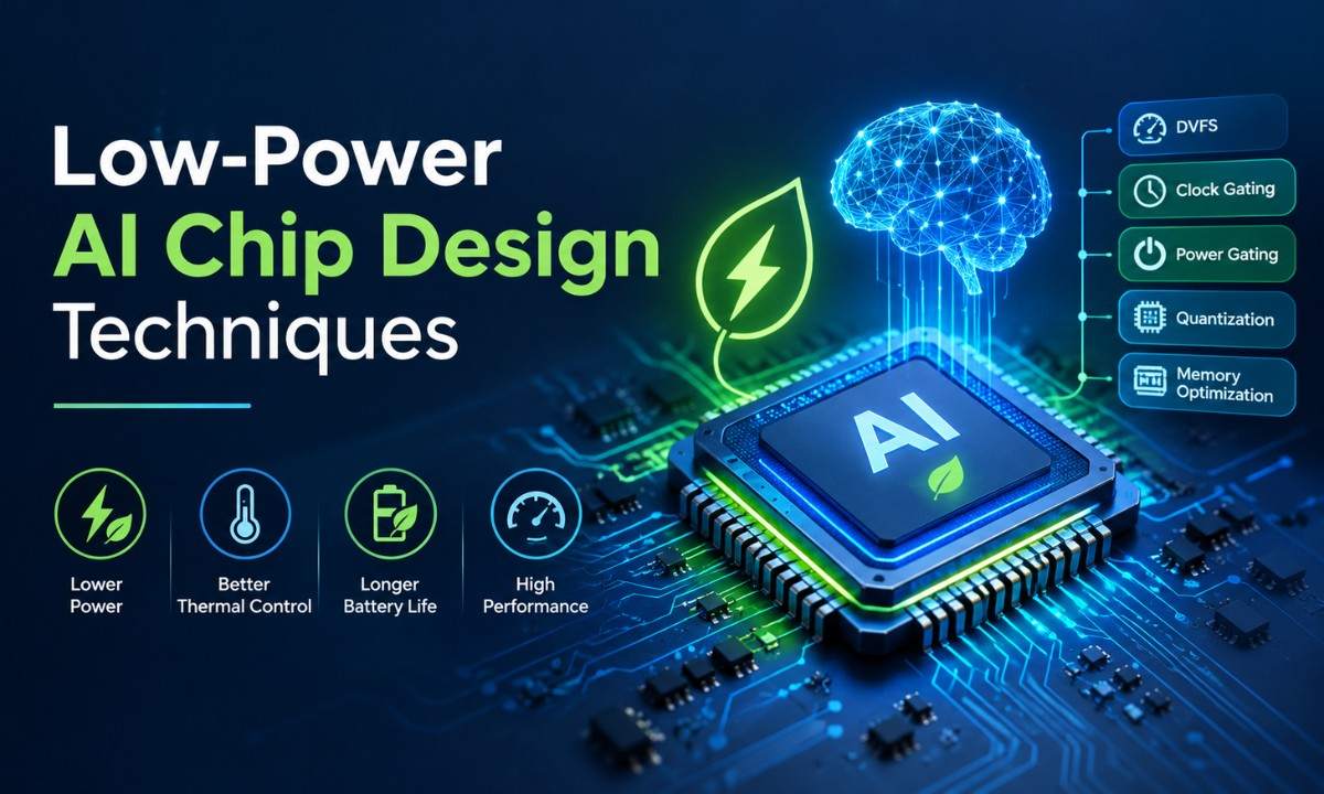
Artificial Intelligence (AI) is transforming industries such as healthcare, automotive engineering, robotics, and consumer electronics. From smartphones to autonomous vehicles, AI applications require powerful computing capabilities to process large amounts of data. However, increasing computational demands can lead to higher power consumption, heat generation, and reduced battery life. This makes Low-Power AI Chip Design Techniques an important area of research in Very Large-Scale Integration (VLSI) design.
Low-power AI chip design focuses on developing energy-efficient hardware that performs AI computations while minimizing unnecessary power consumption. Techniques such as Dynamic Voltage and Frequency Scaling (DVFS), clock gating, power gating, quantization, and memory optimization help improve hardware efficiency.
Understanding these techniques is valuable for electronics engineers and VLSI students exploring semiconductor technology. At Takeoff Edu Group, learning about emerging technologies such as energy-efficient AI hardware helps connect theoretical VLSI concepts with practical engineering applications. As AI adoption continues to grow, low-power chip design remains essential for developing efficient and reliable computing systems.
What Is Low-Power AI Chip Design?
Low-power AI chip design is the process of developing integrated circuits that execute artificial intelligence workloads while reducing energy consumption and managing heat generation. It combines circuit optimization, hardware architecture, and AI model optimization to balance power, performance, and area.
AI chips perform operations such as matrix multiplication, vector processing, and neural network inference. These computations require processing units, memory, and interconnections, all of which contribute to power consumption.
The three major components of chip power consumption are:
- Dynamic power: Power consumed when circuit signals switch between logic states.
- Static power: Power associated with leakage currents when transistors are not actively switching.
- Short-circuit power: Power consumed briefly when transistor networks conduct simultaneously during switching transitions.
Dynamic power can be estimated using the following equation:
P_dynamic = α × C × V² × f
Here, α represents switching activity, C represents effective capacitance, V represents supply voltage, and f represents operating frequency.
Reducing supply voltage, switching activity, or capacitance can help lower dynamic power consumption.
Why Is Low-Power AI Chip Design Important?
Low-power AI chip design is important because it helps hardware operate efficiently within energy, battery, and thermal constraints.
1. Reduced Energy Consumption
AI workloads require substantial computation. Energy-efficient hardware reduces unnecessary switching and improves computational efficiency, helping lower the energy required to execute AI operations.
2. Improved Battery Life
Smartphones, wearables, and IoT devices often operate under strict battery constraints. Low-power AI processors support applications such as voice recognition, image processing, and sensor analysis while managing energy usage.
3. Better Thermal Management
Electrical power consumed by a chip generates heat. Excessive heat can affect reliability and cause processors to reduce performance. Power optimization helps manage temperature and cooling requirements.
4. Efficient Edge AI Computing
Edge AI processes data locally on devices rather than relying entirely on cloud servers. Energy-efficient AI chips make local processing more practical for smart cameras, robotics, industrial monitoring, and connected devices.

Top Low-Power AI Chip Design Techniques
Engineers apply several techniques at the circuit, architecture, and AI model levels to reduce power consumption.
1. Dynamic Voltage and Frequency Scaling (DVFS)
Dynamic Voltage and Frequency Scaling adjusts a processor's supply voltage and operating frequency according to workload requirements.
During demanding tasks, a processor may need a higher frequency to meet performance targets. During lighter workloads, reducing frequency and, where supported, supply voltage can reduce power consumption.
Since dynamic power depends on the square of supply voltage, voltage reduction can significantly improve energy efficiency.
DVFS is commonly relevant to mobile processors, embedded systems, and edge AI devices. Designers must balance power savings against processing speed and timing requirements.
2. Clock Gating
Clock gating reduces dynamic power by disabling clock signals to inactive circuit blocks.
Digital circuits use clock signals to coordinate operations in registers and other sequential components. When a circuit block is inactive, its clock may continue switching unnecessarily.
Clock gating prevents these unnecessary transitions by stopping the clock to selected blocks until they are needed again.
For example, an AI accelerator containing multiple processing units can disable the clock to an unused unit while other units continue operating.
Key benefit: Clock gating reduces unnecessary switching activity and helps minimize dynamic power consumption.
3. Power Gating
Power gating reduces leakage power by disconnecting the supply voltage from selected circuit blocks when they are not required.
It is useful in systems containing hardware components that remain inactive for extended periods. Examples include standby processing units and unused peripheral circuits.
Power gating requires careful consideration of power switches, isolation cells, state retention, and wake-up delays.
Key benefit: Power gating helps reduce power consumption in inactive circuit blocks, particularly leakage power.
4. Quantization and Reduced-Precision Computing
Quantization reduces the numerical precision used by an AI model. For example, a model using 32-bit floating-point values may be converted to use 8-bit integer values when supported by the model and target hardware.
Lower precision can reduce memory requirements and data movement while enabling more efficient computation on compatible AI accelerators.
However, quantization can affect model accuracy. Engineers must evaluate the trade-offs between accuracy, performance, memory usage, and energy consumption.
This technique is particularly useful for edge AI devices and specialized neural network processors.
5. Memory and Data-Movement Optimization
Data movement between memory and processing units can consume significant energy in AI workloads.
Memory optimization techniques aim to reduce unnecessary transfers and improve data reuse. Common approaches include:
- On-chip memory optimization: Keeping frequently used data closer to processing units.
- Data reuse: Reusing weights and intermediate results to reduce repeated memory accesses.
- Efficient memory hierarchies: Organizing storage to reduce costly external memory transfers.
- Processing-in-memory: Exploring architectures that perform selected computations within or near memory.
These approaches help reduce data-transfer overhead and improve the energy efficiency of AI hardware.
6. Hardware Architecture and Circuit-Level Optimization
AI chip efficiency also depends on hardware architecture and circuit implementation.
Application-specific integrated circuits (ASICs) and specialized AI accelerators can be designed for particular workloads, potentially improving energy efficiency compared with less specialized implementations.
At the circuit level, engineers optimize transistor sizing, logic structures, switching activity, capacitance, and interconnections.
These design decisions influence Power, Performance, and Area (PPA), three important metrics used to evaluate VLSI implementations. Designers must balance all three according to the application's requirements.
Role of VLSI Design in Energy-Efficient AI Chips
Very Large-Scale Integration (VLSI) enables engineers to integrate large numbers of transistors into compact integrated circuits. It provides the foundation for developing processors, memory systems, and specialized AI hardware.
Low-power optimization is important throughout the VLSI design flow.
- RTL design: Engineers develop hardware descriptions using languages such as Verilog and SystemVerilog, with attention to unnecessary switching and efficient logic.
- Logic synthesis: Synthesis tools convert RTL into gate-level circuits and optimize the design according to power, performance, and area constraints.
- Physical design: Placement, routing, clock distribution, and power delivery influence circuit capacitance, timing, and power consumption.
- Power analysis and verification: Engineers estimate power under specified workloads and verify that clock gating, power gating, and other low-power features operate correctly.
Considering power consumption throughout these stages helps engineers develop efficient and reliable AI chips.

Applications of Low-Power AI Chip Design
Low-power AI chip design supports several industries.

Challenges in Low-Power AI Chip Design
Despite its advantages, low-power AI chip design involves several technical challenges.
Balancing power and performance: Lower voltage and frequency can reduce power but may affect processing speed and timing.
Maintaining AI accuracy: Quantization and model optimization may affect inference accuracy, requiring careful evaluation.
Managing leakage power: Leakage depends on semiconductor technology, transistor characteristics, and operating conditions.
Reducing memory bottlenecks: Frequent data transfers can increase energy consumption, making memory architecture and data reuse important.
Meeting area and thermal constraints: Additional power-management circuits can increase design complexity and chip area.
Engineers must consider these factors together to achieve an effective balance between energy efficiency, performance, and reliability.
Future Trends in Energy-Efficient AI Hardware
Several developing technologies are influencing the future of low-power AI chip design.
- AI hardware and software co-design: Optimizing AI models and hardware together to improve energy efficiency and performance.
- Specialized AI accelerators: Developing hardware tailored to particular AI operations.
- Processing-in-memory: Exploring ways to reduce energy-intensive data movement.
- Neuromorphic computing: Investigating alternative architectures inspired by aspects of biological neural systems.
- Efficient edge AI: Developing processors capable of running AI workloads within the power constraints of connected and portable devices.
These approaches offer opportunities for improving hardware efficiency, although their benefits depend on the application and implementation maturity.

Conclusion
Low-Power AI Chip Design Techniques play an important role in developing energy-efficient AI hardware for modern computing systems. Techniques such as DVFS, clock gating, power gating, quantization, memory optimization, and specialized AI architectures help engineers reduce power consumption while balancing performance, area, and reliability.
As AI applications expand across healthcare, robotics, automotive systems, IoT, and edge computing, low-power VLSI design will remain an important engineering discipline. Understanding circuit optimization, AI accelerators, and power-aware hardware development can help students and engineers build a strong foundation in semiconductor technology.
At Takeoff Edu Group, exploring Low-Power AI Chip Design Techniques supports technical learning and encourages a deeper understanding of emerging VLSI technologies. By combining efficient circuit design, intelligent hardware architecture, and AI model optimization, engineers can contribute to more energy-efficient and reliable computing systems.
FAQs
1. What are low-power AI chip design techniques?
Low-power AI chip design techniques reduce the energy consumption of AI hardware. Examples include DVFS, clock gating, power gating, quantization, memory optimization, and specialized hardware architectures.
2. What is the difference between clock gating and power gating?
Clock gating disables clock signals to reduce unnecessary switching and dynamic power. Power gating disconnects the supply voltage from selected circuit blocks to reduce their power consumption, particularly leakage power, while inactive.
3. Why is low-power VLSI design important?
Low-power VLSI design helps processors operate within energy and thermal constraints. It is particularly important for mobile devices, IoT systems, embedded hardware, and edge AI applications.
4. How does quantization improve AI hardware efficiency?
Quantization reduces the numerical precision used by AI models. When supported by the hardware, it can reduce memory requirements and improve computational efficiency, although accuracy must be evaluated.
5. How can engineers reduce power consumption in AI chips?
Engineers use DVFS, clock gating, power gating, and quantization to reduce AI chip power consumption. These techniques improve energy efficiency while maintaining performance.
 Hardware Acceleration for Generative AI Models: VLSI Design and Future Trends
 Design and Implementation of Energy-Efficient AI Processors Using VLSI Technology
 FPGA vs ASIC for AI Applications: Which Is Better for AI Workloads?
 AI Accelerators in Modern VLSI: Future of Semiconductor Hardware
 Design and Analysis of Multi-Protocol Conversion Unit for SPI, I2C and UART
 Design of Polar Codes in 5G New Radio
 Design & Study the Performance of CMOS Based Ring Oscillator for 5G Mobile Communication
 Top IEEE VLSI Engineering Projects For Final Year Students with Source Code
 Best VLSI Projects for ECE Students
 Top 7 Transistor Logic Projects for Engineering
 Top 10 Low Power VLSI Projects
 Top 5 Nano Technology Projects using VLSI
 Top 6 Communications Projects for Students
 Top 7 Projects on DSP Core
 Top 5 Projects on Arithmetic Core
 Top 7 Projects on Finite State Machines
 Top 10 Projects on Cadence EDA Tool
 FPGA Final Year Projects for Electronics Students
 Verilog Projects for ECE
 VLSI Project Ideas for Engineering
 VLSI Mini Projects for ECE Department Students
 VLSI Projects for Final Year















 Paper Publishing