Objective
1. Design FPGA-Based Controller for Dot Matrix Display • Implement the control logic for a dot matrix LED display using FPGA. • Generate row and column scanning signals (multiplexing) efficiently to drive the matrix. 2. Character / Pattern Generation • Create a memory (e.g., ROM or block RAM) on the FPGA to store predefined dot patterns. • Design logic to read from this memory and output correct bit patterns to display the desired image or text.
Abstract
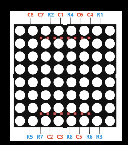
The Dot Matrix using FPGA board is a display system that uses an 8x8 matrix of LEDs to display text or simple graphics. The prototype utilizes Basys 3 FPGA Trainer board, which allows for flexible and efficient programming of the display system. It involves designing and implementing the hardware and software components of the display system, including the LED matrix driver circuit, FPGA board interface, and communication protocol. The hardware core is designed in Verilog, a hardware description language commonly used for FPGA programming. The 8x8 dot matrix is implemented using the 1088AS module which is interfaced with the FPGA to successfully run the system. A dot matrix cannot display the entire alphabet letter at once, so to display the letter in the form of 8x8 lines, the clock frequency of the proposed system is reduced to refresh all 8 columns 1000 times per second. The refresh rate of each column to display letters is 125 Hz. The completed proposed dot matrix display system will be a more secure, high-performance computing and cost-effective solution for displaying text and graphics. It can be useful in various applications, including signage, advertising, and information display purposes. This paper also demonstrates the use of FPGA technology where we can design a cost-effective system for the mass production of display boards than the embedded based solutions which are available in the market.
Keywords:- Verilog, dot matrix,prototype
NOTE: Without the concern of our team, please don't submit to the college. This Abstract varies based on student requirements.
Block Diagram
Specifications
Specifications:
Software Requirements:
· Xilinx ISE14.7 Suite/Vivado2018.3 Tool.
· HDL: Verilog.
Hardware Requirements:
· Microsoft® Windows XP.
· Intel® Pentium® 4 processor or Pentium 4 equivalent with SSE support.
· 512 MB RAM.
· 100 MB of available disk space.
Learning Outcomes
Learning Outcomes:
• Basics of Digital Electronics
• FPGA design Flow
• Introduction to Verilog Coding
• Different modeling styles in Verilog
o Data Flow modeling
o Structural modeling
o Behavioral modeling
o Mixed level modeling
• Drawbacks of existing methods
• Applications in real time
• Xilinx ISE 14.7/Xilinx Vivado for design and simulation
• Generation of Netlist
• Solution providing for real time problems
• Project Development Skills:
o Problem Analysis Skills
o Problem Solving Skills
o Logical Skills
o Designing Skills
o Testing Skills.
o Debugging Skills.
o Presentation Skills.
o Thesis Writing Skills


Related Projects
 Paper Publishing

Request Call Back
Would you like to receive a free callback now?
Choose the best time for callback:
Leave your message and we will contact you as soon as possible

6-2-85/B, Old Maternity Hospital Road, Thyagaraja Nagar, Tirupati, Andhra Pradesh – 517501
+91 9030333433
+91 9393939065
0877-2261612

Disclaimer - Takeoff Edu Group Projects are not associated or affiliated with IEEE in any way. The IEEE Projects mentioned here are mentioned in the context of student projects, whose ideas are derived from IEEE publications, not projects of or by IEEE.