Design of Asynchronous FIFO with Adjustable Input-Output Bit Width Based on Verilog
Objective
Optimized for High-Speed Data Transfer • The design aims to maintain high-speed performance even when performing bit-width conversion. • Ensuring that the FIFO’s control logic and memory structure do not become a bottleneck in high-throughput scenarios.
Abstract
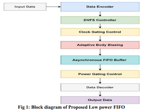
Investigating low-power design methodologies for asynchronous FIFOs is crucial for developing energy-efficient digital systems. This paper explores dynamic voltage and frequency scaling (DVFS), power gating, adaptive body biasing, clock gating, and data encoding techniques to reduce power consumption while maintaining performance in FIFO designs. DVFS adjusts voltage and frequency dynamically based on workload, optimizing power usage. Power gating selectively turns off inactive components to minimize static power dissipation. Adaptive body biasing optimizes transistor characteristics for power and performance trade-offs. Clock gating and data encoding techniques further reduce dynamic power by disabling clock signals to idle parts and minimizing data transitions. These methodologies are integrated into asynchronous FIFO architectures to achieve significant power savings, making them ideal for low-power applications without compromising functionality or performance. Experimental results demonstrate the effectiveness of these techniques in reducing power consumption while ensuring efficient data handling. This research contributes to advancing energy-efficient design practices in asynchronous FIFOs and lays a foundation for developing power-aware digital systems.
Keywords: Power gating, Clock gating, Data encoding, Body biasing, Static power
NOTE: Without the concern of our team, please don't submit to the college. This Abstract varies based on student requirements.
Block Diagram
Specifications
Software Requirements
- Xilinx Vivado Design Suite (2020.2 or later)
- Verilog HDL for RTL design and implementation
- Vivado Simulator (XSIM) for functional and timing verification
- MATLAB (optional) for GPR data preprocessing, noise modeling, and result validation
Hardware Requirements
- Microsoft® Windows 10 / Windows 11 (64-bit)
- Intel® Core™ i5 / i7 Processor or equivalent
- Minimum 8 GB RAM
- Minimum 500 MB free disk space
Learning Outcomes
Understand the fundamentals of asynchronous FIFO architectures, including clock domain crossing (CDC) challenges and metastability issues.
Gain knowledge of Gray code pointers, synchronizers, and full/empty flag generation for reliable asynchronous data transfer.
Learn to design and implement parameterized FIFOs with adjustable input and output bit widths using Verilog HDL.
Analyze data packing and unpacking techniques required for handling different read/write data widths.
Develop skills in validating FIFO functionality through simulation and timing analysis under independent clock domains.
Evaluate performance metrics such as latency, throughput, area, and power consumption for different FIFO configurations.
Acquire practical experience in synthesizing and verifying asynchronous FIFO designs using Xilinx Vivado.


Related Projects
 Paper Publishing

Request Call Back
Would you like to receive a free callback now?
Choose the best time for callback:
Leave your message and we will contact you as soon as possible

6-2-85/B, Old Maternity Hospital Road, Thyagaraja Nagar, Tirupati, Andhra Pradesh – 517501
+91 9030333433
+91 9393939065
0877-2261612

Disclaimer - Takeoff Edu Group Projects are not associated or affiliated with IEEE in any way. The IEEE Projects mentioned here are mentioned in the context of student projects, whose ideas are derived from IEEE publications, not projects of or by IEEE.