Design and Implementation of SRAM on FPGA and Verification Using UVM
Objective
The objective of this project is to design and implement a Static Random Access Memory (SRAM) on an FPGA platform to achieve high-speed and efficient data storage. It focuses on developing a memory architecture with optimized area and power utilization. The design will be synthesized, implemented, and tested on FPGA hardware to verify its functionality and performance. Universal Verification Methodology (UVM) is used to create a reusable and robust verification environment. The goal is to ensure the correctness, reliability, and efficiency of the SRAM design through functional and timing verification
Abstract
Abstract:
This research focuses on the design, verification, and implementation of a 6T SRAM using HDL, UVM, and FPGA for performance optimization. A reusable UVM testbench ensures thorough verification of read and write operations, while coverage-driven verification verify all possible scenarios. System Verilog assertions enhance design correctness. The 6T SRAM model is simulated and synthesized using Vivado for functional verification. Additionally, a comparative analysis of 6T SRAM, Dual port 6T SRAM (DSRAM), and Pseudo static RAM (P6T SRAM) is conducted, focusing on power consumption, speed, and area utilization. The aims to develop an efficient memory architecture for high-speed, low-power applications, ensuring reliability and improved performance in digital systems.NOTE: Without the concern of our team, please don't submit to the college. This Abstract varies based on student requirements.
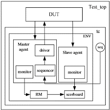
Block Diagram
Specifications
Software Requirements:
· Xilinx ISE14.7 Suite/Vivado2018.3 Tool.
· HDL: Verilog.
Hardware Requirements:
· Microsoft® Windows XP.
· Intel® Pentium® 4 processor or Pentium 4 equivalent with SSE support.
· 512 MB RAM.
· 100 MB of available disk space.
Learning Outcomes
1. Understanding of SRAM architecture and memory operations.
2. Hands-on experience with FPGA-based SRAM implementation.
3. Knowledge of UVM components and verification flow.
4. Skills in writing SystemVerilog assertions and functional coverage.
5. Experience with industry-standard verification practices.
6. Ability to design and verify scalable and reusable memory modules.
Demo Video


Request for Video
Related Projects
 Paper Publishing
Request Call Back
Would you like to receive a free callback now?
Choose the best time for callback:
Leave your message and we will contact you as soon as possible

6-2-85/B, Old Maternity Hospital Road, Thyagaraja Nagar, Tirupati, Andhra Pradesh – 517501
+91 9030333433
+91 9393939065
0877-2261612

Disclaimer - Takeoff Edu Group Projects are not associated or affiliated with IEEE in any way. The IEEE Projects mentioned here are mentioned in the context of student projects, whose ideas are derived from IEEE publications, not projects of or by IEEE.