Virtex 7 FPGA Implementation of 256 Bit Key AES Algorithm with Key Schedule and Sub Bytes Block Optimization
Also Available Domains Xilinx Vivado|Xilinx ISE
Objective
The main objective of this paper is to improve the security by extending the cipher key size into 256 bit key AES algorithm and applied selective transformation for optimization.
Abstract
Information security has a major role in the development next generation communication system, where more randomization in the secret key is required for improved security without adding any complexity over existing cryptography algorithms. In the recent years Symmetric key algorithms like Advanced Encryption Standard (AES) is widely used in many network security applications. In Symmetric key algorithms hierarchical physical and key based transformation blocks are used for both encryption and decryption process. Hardware optimization also plays a vital role for reducing the computational complexity and power consumption rate of AES core. In this paper 256-bit AES algorithm is proposed with optimized Key schedule and Sub bytes blocks for Area and Power optimization. Here the hardware optimization is accomplished by reusing the S-box block and share the common resource for all internal operations for only 32-bit operations rather than 128-bit operations. The proposed model allows to re-use the same hardware in a pipelined fashion. Recently, many key management schemes have been proposed, each with its own particular strengths, weaknesses, and applications under certain circumstances. In addition to this paper also proposes an extension of a dynamic key extraction in cryptosystem which can maximize the randomness by adding outer layer security. Finally, the performance metrics like randomness, design complexity, reliability, and discriminative properties are compared with existing works. Through Experimental results the metrics of proposed key generation like randomness, distinctiveness.
NOTE: Without the concern of our team, please don't submit to the college. This Abstract varies based on student requirements.
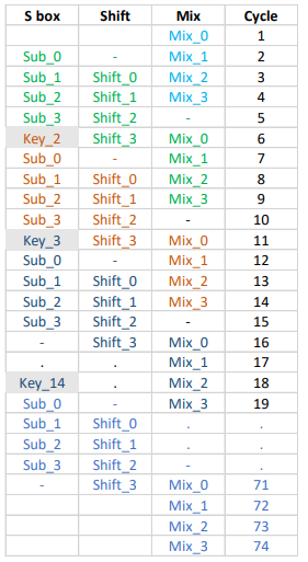
Block Diagram
Specifications
Software Requirements:
- Xilinx ISE/Xilinx Vivado Tool
- HDL: Verilog
Hardware Requirements:
- Microsoft® Windows XP,
- Intel® Pentium® 4 processor or Pentium 4 equivalent with SSE support
- 512 MB RAM
- 100 MB of available disk space
Learning Outcomes
- Basics of Digital Electronics
- FPGA design Flow
- Introduction to Verilog Coding
- Different modeling styles in Verilog
- Data Flow modeling
- Structural modeling
- Behavioral modeling
- Mixed level modeling
- Concept of Cryptography systems
- Importance of Crypto systems
- Drawbacks of existing methods
- Introduction to Advanced Encryption standard (AES)
- Knowledge on pipelining concept
- Knowledge on Symmetric, Asymmetric and Hash functions
- Applications of AES in real time
- Scope of AES concept in today’s world
- Applications in real time
- Xilinx ISE 14.7/Xilinx Vivado for design and simulation
- Generation of Netlist
- Solution providing for real time problems
- Project Development Skills:
- Problem Analysis Skills
- Problem Solving Skills
- Logical Skills
- Designing Skills
- Testing Skills
- Debugging Skills
- Presentation Skills
- Thesis Writing Skills
Demo Video


Request for Video
Related Projects
 Paper Publishing
Request Call Back
Would you like to receive a free callback now?
Choose the best time for callback:
Leave your message and we will contact you as soon as possible

6-2-85/B, Old Maternity Hospital Road, Thyagaraja Nagar, Tirupati, Andhra Pradesh – 517501
+91 9030333433
+91 9393939065
0877-2261612

Disclaimer - Takeoff Edu Group Projects are not associated or affiliated with IEEE in any way. The IEEE Projects mentioned here are mentioned in the context of student projects, whose ideas are derived from IEEE publications, not projects of or by IEEE.