Rapid Low power Voltage level shifter Utilizing Regulated Cross Coupled Pull Up Network
Also Available Domains Low Power VLSI|Cadence EDA
Abstract
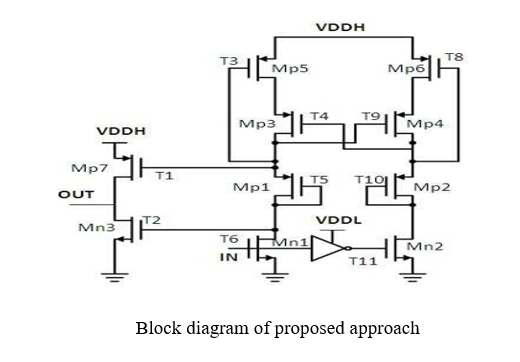
In this concise, ultralow power and high speed voltage or logic LS circuit is introduced. With the help of regulated cross coupled structure in the pull up region the power utilized by the circuit is considerably decreased and speed of the circuit is also increased. The LS can convert the input logic levels or voltages below the VTH of the transistor to the higher acceptable levels. A LS requires less area because it consists of less number of components which makes it fit for low power and high speed applications, for example implantable clinical gadgets and remote sensor organizations.
NOTE: Without the concern of our team, please don't submit to the college. This Abstract varies based on student requirements.
Block Diagram

Specifications
Software Requirements:
- Tanner EDA
- Technology files: 180nm
Hardware Requirements:
- Microsoft® Windows XP
- Intel® Pentium® 4 processor or Pentium 4 equivalent with SSE support
- 512 MB RAM
- 100 MB of available disk space
Learning Outcomes
- Introduction to Differential cascaded voltage switch
- Knowledge on Level shifters
- Knowledge on current mirror circuits
- Knowledge on Regulated cross coupled structures
- Basics of cross coupled pull up & pull down networks
- Limitations & Advantages
- Importance of Transistors
- MOS Fundamentals
- NMOS/PMOS/CMOS Technologies
- How to design circuits using Transistor logic?
- Transistor level design for Level shifter
- How to design Level shifter with RCC pull up network
- Introduction to Analog Electronics
- Importance of Cross coupled comparators
- Scope of cross coupled networks in today’s world
- Applications in Real time.
- Tanner EDA tool for design and simulation
- Solution providing for real time problems
- Project Development Skills:
- Problem Analysis Skills
- Problem Solving Skills
- Logical Skills
- Designing Skills
- Testing Skills
- Debugging Skills
- Presentation skills
- Thesis Writing Skills


 Paper Publishing
