Power optimization in configurable ALU using blend of techniques
Objective
The main objective of this project is to reduce the power dissipation for the design of ALU using different configurations of Clock gating Technique.
Abstract
NOTE: Without the concern of our team, please don't submit to the college. This Abstract varies based on student requirements.
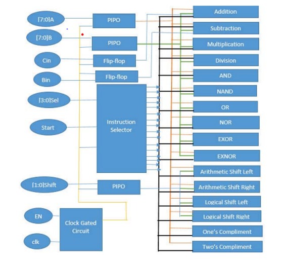
Block Diagram
Specifications
Software Requirements:
· Xilinx Vivado Tool
· HDL: Verilog
Hardware Requirements:
· Microsoft® Windows XP
· Intel® Pentium® 4 processor or Pentium 4 equivalent with SSE support
· 512 MB RAM
· 100 MB of available disk space
Learning Outcomes
Understanding voltage level shifting: Gain knowledge about the concept of voltage level shifting and its importance in electronic systems. Learn about the challenges and considerations involved in converting voltage levels between different supply voltages.
Familiarity with dual-supply applications: Explore the specific requirements and characteristics of dual-supply applications. Understand why and when dual-supply configurations are used and the benefits they offer in certain scenarios.
Knowledge of existing voltage level shifting techniques: Study various existing techniques and approaches for voltage level shifting in dual-supply applications. Understand their advantages, limitations, and trade-offs in terms of speed, power efficiency, area utilization, and performance.
Analyzing the high-speed requirement: Gain insights into the need for high-speed voltage level shifters in certain applications. Understand the implications of high-speed requirements on power consumption, signal integrity, and overall system performance.
Investigating power efficiency: Explore the significance of power efficiency in voltage level shifting designs. Learn about low-power design techniques, such as power gating, supply voltage scaling, and optimizing circuit topologies, to achieve power-efficient operation.
Designing a high-speed and power-efficient voltage level shifter: Apply the knowledge gained to design a voltage level shifter that meets the requirements of high speed and power efficiency in dual-supply applications. Understand the design considerations, trade-offs, and challenges involved in achieving these objectives.
Simulation and analysis: Utilize simulation tools and techniques to validate the design, analyze its performance, and assess its speed and power efficiency. Gain hands-on experience in simulating and analyzing the behavior of voltage level shifters under different operating conditions.
Evaluating trade-offs: Develop the ability to evaluate trade-offs between speed, power efficiency, area utilization, and other performance metrics. Understand how design choices and optimization strategies impact these trade-offs and make informed decisions based on the specific requirements of the application.
Documentation and reporting: Develop effective communication skills by documenting the design process, results, and findings in a clear and concise manner. Prepare a comprehensive report summarizing the design, implementation, and performance analysis of the high-speed and power-efficient voltage level shifter.
Critical thinking and problem-solving: Enhance critical thinking and problem-solving skills by identifying and addressing challenges and limitations in the design process. Explore alternative solutions, evaluate their feasibility, and propose improvements or optimizations to enhance the speed and power efficiency of the voltage level shifter


 Paper Publishing

Request Call Back
Would you like to receive a free callback now?
Choose the best time for callback:
Leave your message and we will contact you as soon as possible

6-2-85/B, Old Maternity Hospital Road, Thyagaraja Nagar, Tirupati, Andhra Pradesh – 517501
+91 9030333433
+91 9393939065
0877-2261612

Disclaimer - Takeoff Edu Group Projects are not associated or affiliated with IEEE in any way. The IEEE Projects mentioned here are mentioned in the context of student projects, whose ideas are derived from IEEE publications, not projects of or by IEEE.