Performance Evaluation of 6T-Sram in Sub-3 nm Complementary Fet
Objective
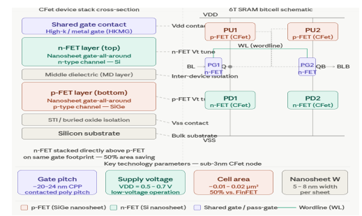
This work presents a comprehensive performance evaluation of a 6-transistor (6T) SRAM cell implemented using sub-3 nm Complementary Field-Effect Transistor (CFET) technology. As traditional CMOS and FinFET scaling approaches its physical and electrostatic limits, CFET emerges as a promising device architecture by vertically stacking nMOS and pMOS transistors to achieve higher density and superior gate control
Abstract
This work presents a comprehensive performance evaluation of a 6-transistor (6T) SRAM cell implemented using sub-3 nm Complementary Field-Effect Transistor (CFET) technology. As traditional CMOS and FinFET scaling approaches its physical and electrostatic limits, CFET emerges as a promising device architecture by vertically stacking nMOS and pMOS transistors to achieve higher density and superior gate control.
In this work, a conventional 6T SRAM topology is adapted to CFET-based devices and analyzed under ultra-scaled conditions. Key performance metrics such as static noise margin (SNM), read stability, write ability, leakage power, and access delay are evaluated. The design aims to address major scaling challenges including increased leakage, reduced noise margins, and variability effects.
Simulation results demonstrate that the CFET-based SRAM cell achieves improved area efficiency, reduced leakage power, and enhanced electrostatic control compared to conventional FinFET-based SRAM designs, while maintaining reliable read and write operations. The proposed approach is well-suited for next-generation high-density, low-power memory applications in advanced VLSI systems.
Keywords
6T SRAM, CFET, Sub-3 nm Technology, Static Noise Margin (SNM), Low Power, Advanced VLSI, Memory Design
NOTE: Without the concern of our team, please don't submit to the college. This Abstract varies based on student requirements.
Block Diagram
Specifications
· Tool Used: Cadence EDA tools for schematic and simulation
· Technology Node:180nm CMOS process.
· Design Elements: complementary compound push–pull pair (PMOS + NMOS), input matching network, L1 & L2 (0.5 pH–10 pH) inductors, high-value output load (RL, 100 kΩ–1 MΩ), biasing/level-shift network, feedback/compensation path, input/output coupling and decoupling capacitors, thermal-stabilization circuitry, and symmetric/layout considerations for reduced mismatch
· Optimization Goal: minimize circuit complexity and parasitics (transistor and passive count) while preserving ultra-wideband large-signal gain, low output noise, high temperature stability, and linearity across the desired cutoff range (e.g., maintain cutoff from ≈18.21 kHz up to hundreds of GHz in simulation) with low power consumption (~69 mW)v
Learning Outcomes
Understanding of CFET Device Architecture
• Knowledge of 6T SRAM Cell Operation
• Analysis of Scaling Challenges in Nanoelectronics
• Evaluation of Stability using SNM
• Low-Power Memory Design Techniques
• Exposure to Advanced Sub-3 nm Technologies


 Paper Publishing

Request Call Back
Would you like to receive a free callback now?
Choose the best time for callback:
Leave your message and we will contact you as soon as possible

6-2-85/B, Old Maternity Hospital Road, Thyagaraja Nagar, Tirupati, Andhra Pradesh – 517501
+91 9030333433
+91 9393939065
0877-2261612

Disclaimer - Takeoff Edu Group Projects are not associated or affiliated with IEEE in any way. The IEEE Projects mentioned here are mentioned in the context of student projects, whose ideas are derived from IEEE publications, not projects of or by IEEE.