Optimal Design of Reversible Parity Preserving New Full Adder Full Subtractor
Objective
The proposed method require less complexity, less hardware, minimum number of gates, minimum number of garbage inputs and minimum number of constant inputs than existing methods.
Abstract
The widely using CMOS technology implementing with irreversible logic will hit a scaling limit beyond 2020 and the major limiting factor is increased power dissipation. The irreversible logic is replaced by reversible logic to decrease the power dissipation. The devices implemented with reversible logic gates will have demand for the upcoming future computing technologies as they consumes less power. Reversible logic has applications in Low Power VLSI, Quantum Computing, Nanotechnology and Optical computing. This paper proposes the design of a optimal fault tolerant Full adder / Full subtractor. For this logic circuit input parity and output parity is same hence it is called parity preserving circuit. The proposed method require less complexity, less hardware, minimum number of gates, minimum number of garbage inputs and minimum number of constant inputs than existing methods.
NOTE: Without the concern of our team, please don't submit to the college. This Abstract varies based on student requirements.
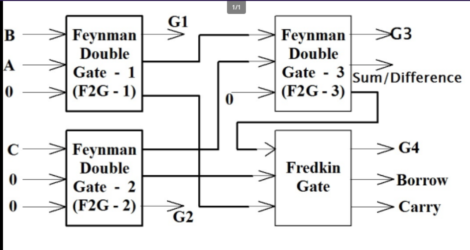
Block Diagram
Specifications
System Configuration:-
In the hardware part a normal computer where Xilinx ISE 14.3 software can be easily operated is required, i.e., with a minimum system configuration
Hardware requirement
Processor - Pentium –III
Speed - 1.1 GHz
RAM - 1 GB (min)
Hard Disk - 40 GB
Floppy Drive - 1.44 MB
Key Board - Standard Windows Keyboard
Mouse- Two or Three Button Mouse
Monitor - SVGA
Software requirements
v Operating System :Windows95/98/2000/XP/Windows7
v Front End : Modelsim 6.3 for Debugging and Xilinx 14.3 for Synthesis and Hard Ware Implementation
v This software’s where Verilog source code can be used for design implementation.
Learning Outcomes
Understanding Reversible Logic: Gain a deep understanding of reversible logic and its significance in the field of digital circuit design. Learn about the principles, advantages, and challenges associated with reversible logic.
Knowledge of Full Adders/Subtractors: Develop a comprehensive understanding of conventional full adders and full subtractors, including their architectures, functionality, and limitations. Study different design approaches and their trade-offs.
Exploring Reversible Full Adder/Subtractor Designs: Explore various existing reversible full adder and full subtractor designs. Understand their working principles, efficiency, and limitations. Compare and contrast different design techniques and analyze their impact on circuit performance.
Analyzing Parity-Preserving Logic: Investigate the concept of parity-preserving logic and its significance in reversible circuit design. Learn how to maintain the parity of signals during the computation and understand the implications of preserving parity.
Design Optimization: Learn techniques for optimizing the design of reversible full adders and full subtractors. Explore methods such as gate-level optimization, transistor-level optimization, and logic synthesis to improve circuit efficiency, power consumption, and area utilization.
Performance Evaluation: Develop the skills to evaluate the performance of reversible full adders and full subtractors. Analyze metrics such as delay, power dissipation, energy consumption, area utilization, and the trade-offs between these parameters.
Research and Innovation: Foster a research-oriented mindset and explore avenues for innovation in the field of reversible circuit design. Stay updated with the latest advancements, emerging technologies, and research publications related to reversible full adders and full subtractors.
Problem-Solving Skills: Enhance problem-solving abilities by tackling complex design challenges and addressing the unique constraints of reversible circuit design. Develop critical thinking skills to overcome obstacles and optimize circuit performance.
Communication and Presentation: Learn to effectively communicate and present research findings, design methodologies, and optimization techniques related to reversible full adders and full subtractors. Develop skills to convey technical information to both technical and non-technical audiences.
Ethical and Professional Considerations: Understand the ethical and professional considerations associated with reversible circuit design. Learn about intellectual property rights, patents, and legal aspects related to innovation in the field. Develop a sense of responsibility and integrity in research and design practices.


 Paper Publishing

Request Call Back
Would you like to receive a free callback now?
Choose the best time for callback:
Leave your message and we will contact you as soon as possible

6-2-85/B, Old Maternity Hospital Road, Thyagaraja Nagar, Tirupati, Andhra Pradesh – 517501
+91 9030333433
+91 9393939065
0877-2261612

Disclaimer - Takeoff Edu Group Projects are not associated or affiliated with IEEE in any way. The IEEE Projects mentioned here are mentioned in the context of student projects, whose ideas are derived from IEEE publications, not projects of or by IEEE.