Low Power Redundant Transition Free TSPC Dual Edge Triggering Flip Flop Using Single Transistor Clocked Buffer
Objective
The main objective of this project is to design the dual triggering flip-flop using STC
Abstract
In the modern graphics processing unit (GPU)/artificial intelligence (AI) era, flip-flop (FF) has become one of the most power-hungry blocks in processors. To address this issue, a novel singlephase-clock dual-edge-triggering (DET) FF using a single-transistor clocked (STC) buffer (STCB) is proposed. The STCB uses a single-clocked transistor in the data sampling path, which completely removes clock redundant transitions (RTs) and internal RTs that exist in other DET designs. Verified by post-layout simulations in 22 nm fully depleted silicon on insulator (FD-SOI) CMOS, when operating at 10% switching activity, the proposed STC-DET outperforms prior state-of-the-art low power DET in power consumption by It also achieves the lowest power-delay-product (PDP) among the DETs.
NOTE: Without the concern of our team, please don't submit to the college. This Abstract varies based on student requirements.
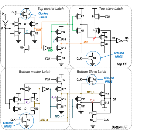
Block Diagram
Specifications
Software Requirements:
Tanner EDA Tool
Technology used:22nm
Minimum Hardware Requirements:
o Microsoft Windows 7
o Intel i3 processor or equivalent
o 4GB RAM
o 100 MB of available disk space
Learning Outcomes
• Basics of Digital Electronics
• VLSI design Flow
• Knowledge of Flip-Flop Principles
• Understanding Timing Considerations
• Timing Analysis and Verification
• Drawbacks of existing methods
• Applications in real time
• Tanner Tool for design and simulation
• Solution providing for real time problems
• Project Development Skills:
o Problem Analysis Skills
o Problem Solving Skills
o Logical Skills
o Designing Skills
Demo Video


Request for Video
Related Projects
 Paper Publishing
Request Call Back
Would you like to receive a free callback now?
Choose the best time for callback:
Leave your message and we will contact you as soon as possible

6-2-85/B, Old Maternity Hospital Road, Thyagaraja Nagar, Tirupati, Andhra Pradesh – 517501
+91 9030333433
+91 9393939065
0877-2261612

Disclaimer - Takeoff Edu Group Projects are not associated or affiliated with IEEE in any way. The IEEE Projects mentioned here are mentioned in the context of student projects, whose ideas are derived from IEEE publications, not projects of or by IEEE.