Low Power, High Performance PMOS Biased Sense Amplifier
Also Available Domains Cadence EDA
Objective
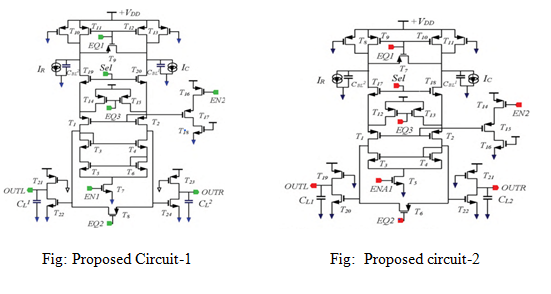
In this paper, two proposed circuits of PMOS-biased sense amplifier is implemented. A fast access time and low power dissipation are achieved with newly developed circuits of sense amplifier for low voltage supply.
Abstract
Abstract: In this paper, PMOS biased sense amplifier is proposed. Sense amplifiers plays a significant role in terms of its recital, functionality and reliability of the memory circuits. The proposed circuit is PMOS biased sense amplifier, which provides very high output impedance and has reduced sense delay and power dissipation and it performs the identical operations as that of conventional circuits. The suggested sense amplifiers overall performance have been simulated and examined using Tanner EDA employing 180 nm library parameters.
NOTE: Without the concern of our team, please don't submit to the college. This Abstract varies based on student requirements.
Block Diagram

Specifications
Software Requirements:
Tanner EDA/Cadence EDA
Technology files: 180nm
Hardware Requirements:
Microsoft® Windows XP
Intel® Pentium® 4 processor or Pentium 4 equivalent with SSE support
512 MB RAM
100 MB of available disk space
Learning Outcomes
Introduction to Sense Amplifiers
Types of Sense Amplifiers
Limitations & Applications.
Introduction to PMOS Biased sense amplifier.
Knowledge on Differential amplifiers
Knowledge on Current Mirror circuits
Importance of Transistors
MOS Fundamentals
NMOS/PMOS/CMOS Technologies
How to design circuits using Transistor logic?
Transistor level design for PMOS Biased Sense Amplifier
How to design Proposed circuits of PMOS Biased sense amplifier
Introduction to Analog Electronics
Importance of Memory units
Scope of Sense Amplifiers in today’s world
Applications in Real time.
Tanner EDA/Cadence Virtuoso tool for design and simulation
Solution providing for real time problems
Project Development Skills:
Problem Analysis Skills
Problem Solving Skills
Logical Skills
Designing Skills
Testing Skills
Debugging Skills
Presentation skills
Thesis Writing Skills


 Paper Publishing
