Low-Cost Multiple Bit Upset Correction In SRAM-based FPGA Configuration Frames
Also Available Domains Xilinx Vivado|Xilinx ISE
Objective
The main objective of this project is to reduce the error correction codes of high overhead to mitigate the MBU in configuration frames by implementing the low cost error correction scheme in SRAM based FPGA configuration frames.
Abstract
Radiation-induced multiple bit upsets (MBUs) are a major reliability concern in Nano scale technology nodes. Occurrence of such errors in the configuration frames of a field programmable gate array (FPGA) device permanently affects the functionality of the mapped design. Periodic configuration scrubbing combined with a low-cost error correction scheme is an efficient approach to avoid such a permanent effect. Existing techniques employ error correction codes with considerably high overhead to mitigate MBUs in configuration frames. In this paper, we present a low-cost error-detection code to detect MBUs in configuration frames as well as a generic scrubbing scheme to reconstruct the erroneous configuration frame based on the concept of erasure codes. The proposed scheme does not require any modification to the FPGA architecture. Implementation of the proposed scheme on a Xilinx Virtex-6 FPGA device shows that the proposed scheme can detect 100% of MBUs in the configuration frames with only 3.3% resource occupation, while the recovery time is comparable with the previous schemes. The effectiveness of the proposed method synthesized and simulated in Xilinx ISE 14.7.
NOTE: Without the concern of our team, please don't submit to the college. This Abstract varies based on student requirements.
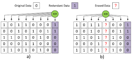
Block Diagram
Specifications
Software Requirements:
- Xilinx ISE 14.7 Tool
- HDL: Verilog
- Microsoft® Windows XP,
- Intel® Pentium® 4 processor or Pentium 4 equivalent with SSE support
- 512 MB RAM
- 100 MB of available disk space
Learning Outcomes
- Basics of Digital Electronics
- FPGA design Flow
- Introduction to Verilog Coding
- Different modeling styles in Verilog
- Data Flow modeling
- Structural modeling
- Behavioral modeling
- Mixed level modeling
- Combinational & Sequential circuits
- Knowledge on Arithmetic circuits
- Study on single cell upsets and multi cell upsets, soft errors
- About SRAM based FPGAs
- Knowledge on Error correction codes
- About architecture of FPGA configuration frames
- Applications of error recovery in FPGA configuration frames in real time
- Xilinx ISE for design and simulation
- Generation of Netlist
- Solution providing for real time problems
- Project Development Skills:
- Problem Analysis Skills
- Problem Solving Skills
- Logical Skills
- Designing Skills
- Testing Skills
- Debugging Skills
- Presentation Skills
- Thesis Writing Skills


 Paper Publishing

Request Call Back
Would you like to receive a free callback now?
Choose the best time for callback:
Leave your message and we will contact you as soon as possible

6-2-85/B, Old Maternity Hospital Road, Thyagaraja Nagar, Tirupati, Andhra Pradesh – 517501
+91 9030333433
+91 9393939065
0877-2261612

Disclaimer - Takeoff Edu Group Projects are not associated or affiliated with IEEE in any way. The IEEE Projects mentioned here are mentioned in the context of student projects, whose ideas are derived from IEEE publications, not projects of or by IEEE.