Integration of Optimized GDI Logic based NOR Gate and Half Adder into PASTA for Low Power & Low Area Applications
Objective
This paper focuses on circuit level optimization to reduce the area and power consumption.
Abstract
Abstract: The utilization of MOS technology is prevalent in VLSI circuits for reducing the number of transistors and achieving low power consumption. This can be accomplished via either circuit level optimization or logical level optimization. This paper focuses on circuit level optimization to reduce the area and power consumption. A conventional complementary static CMOS (CSCMOS) technology is used to design a parallel self-timed adder circuit where the number of NMOS and PMOS transistors is equal. However, this approach requires a large number of transistors, resulting in high area and power consumption. To address this issue, the proposed parallel asynchronous self-time adder (PASTA) technique utilizes modified gate diffusion input (GDI) logic. Additionally, the structure of the XOR gate and half adder are minimized to achieve low area and low power consumption. A comparison between the two techniques is performed, and the results demonstrate that the proposed GDI logic-based PASTA utilizes fewer transistors (area) and has lower power consumption than the existing CSCMOS technique. The functionality of the PASTA circuits is verified through simulations conducted via the tanner tool.
NOTE: Without the concern of our team, please don't submit to the college. This Abstract varies based on student requirements.
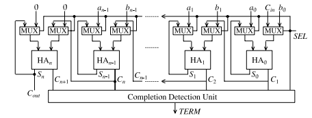
Block Diagram
Specifications
Specifications:
Software Requirements:
· Tool: Tanner EDA
· Technology: 45nm
Hardware Requirements:
· Microsoft® Windows XP
· Intel® Pentium® 4 processor or Pentium 4 equivalent with SSE support
· 512 MB RAM
· 100 MB of available disk space
Learning Outcomes
· Knowledge on Digital Electronics
o Basics of Combinational Circuits
· Introduction to PASTA Adder
· Advantages and Applications of PASTA Adder
· Knowledge on Analog Electronics
o Basics of Transistors & MOSFETs
· Transistor level schematic of PASTA adder
· Simulation of schematic in T-spice.
· Analyzing the waveforms and results
· Scope of PASTA adder in Today’s world.


 Paper Publishing

Request Call Back
Would you like to receive a free callback now?
Choose the best time for callback:
Leave your message and we will contact you as soon as possible

6-2-85/B, Old Maternity Hospital Road, Thyagaraja Nagar, Tirupati, Andhra Pradesh – 517501
+91 9030333433
+91 9393939065
0877-2261612

Disclaimer - Takeoff Edu Group Projects are not associated or affiliated with IEEE in any way. The IEEE Projects mentioned here are mentioned in the context of student projects, whose ideas are derived from IEEE publications, not projects of or by IEEE.