Implementation of Low Power and High Speed Dadda Multiplier using Xor-Xnor cell Based Hybrid Logic Full Adder
Objective
this research presents a novel approach to designing Dadda multipliers using XOR-XNOR cell based hybrid logic full adders, aiming to achieve low power consumption and high speed operation
Abstract
This project presents the design and implementation of a low-power, high-speed Dadda multiplier using XOR-XNOR cell-based hybrid logic full adders. The Dadda multiplier architecture is optimized to reduce critical path delay and minimize power consumption while maintaining high computational accuracy. By incorporating XOR-XNOR hybrid full adder cells, the design efficiently balances speed and energy efficiency, allowing fast arithmetic operations with reduced switching activity. The multiplier is implemented using advanced CMOS technology and analyzed for key performance metrics such as propagation delay, power consumption, area, and overall throughput. Simulation results demonstrate that the proposed multiplier achieves significant improvements in speed and energy efficiency compared to conventional full adder-based designs. The scalable architecture makes it suitable for integration into digital signal processing units, high-speed processors, and other VLSI applications requiring high-performance arithmetic computation.
NOTE: Without the concern of our team, please don't submit to the college. This Abstract varies based on student requirements.
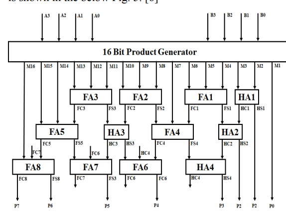
Block Diagram
Specifications
Software Requirements:
• Tool: Cadence
Hardware Requirements:
• Microsoft® Windows XP
• Intel® Pentium® 4 processor or Pentium 4 equivalent with SSE support
• 512 MB RAM
• 100 MB of available disk space
Learning Outcomes
-
Understanding the architecture and operation of Dadda multipliers for high-speed arithmetic computation.
-
Ability to design hybrid logic full adders using XOR-XNOR cells for low-power and high-speed performance.
-
Practical skills in using Cadence Virtuoso and Spectre Simulator for schematic design, simulation, and layout implementation.
-
Knowledge of optimizing critical path delay, power consumption, and transistor count in multiplier circuits.
-
Competence in evaluating performance metrics such as propagation delay, power-delay product (PDP), area, and energy efficiency.
-
Understanding trade-offs between speed, power, and area in VLSI multiplier design.
-
Experience in scalable design techniques for extending 1-bit adder cells to multi-bit multipliers.
-
Ability to perform post-layout simulations and parasitic extraction for accurate performance evaluation.
-
Preparedness to implement energy-efficient, high-speed arithmetic circuits in digital signal processing (DSP) and embedded applications.
-
Enhanced problem-solving skills for designing optimized VLSI arithmetic modules suitable for high-performance computing.
Demo Video


Request for Video
 Paper Publishing
Request Call Back
Would you like to receive a free callback now?
Choose the best time for callback:
Leave your message and we will contact you as soon as possible

6-2-85/B, Old Maternity Hospital Road, Thyagaraja Nagar, Tirupati, Andhra Pradesh – 517501
+91 9030333433
+91 9393939065
0877-2261612

Disclaimer - Takeoff Edu Group Projects are not associated or affiliated with IEEE in any way. The IEEE Projects mentioned here are mentioned in the context of student projects, whose ideas are derived from IEEE publications, not projects of or by IEEE.