Implementation of full adder using pass transistor Logic for low Power VLSI Circuits
Objective
This paper presents a low-power full adder design based on pass-transistor logic (PTL) aimed at achieving reduced power consumption and compact area for energy-efficient VLSI systems. By utilizing pass-transistor logic, the proposed full adder significantly decreases transistor count, internal node capacitance, and switching activity compared to conventional CMOS implementations. The reduced logic depth and simplified signal paths enable faster sum and carry generation while maintaining functional correctness. The proposed PTL-based full adder is implemented in scaled CMOS technology and evaluated in terms of power consumption, propagation delay, area, and power–delay product (PDP).
Abstract
This paper presents a low-power full adder design based on pass-transistor logic (PTL) aimed at achieving reduced power consumption and compact area for energy-efficient VLSI systems. By utilizing pass-transistor logic, the proposed full adder significantly decreases transistor count, internal node capacitance, and switching activity compared to conventional CMOS implementations. The reduced logic depth and simplified signal paths enable faster sum and carry generation while maintaining functional correctness. The proposed PTL-based full adder is implemented in scaled CMOS technology and evaluated in terms of power consumption, propagation delay, area, and power–delay product (PDP). Simulation results demonstrate that the design achieves substantial power savings and improved energy efficiency, particularly under low supply voltage operation. Owing to its compact structure and low-power characteristics, the proposed pass-transistor logic-based full adder is well suited for arithmetic-intensive applications such as multipliers, adders, digital signal processing units, and low-power embedded systems.
KEYWORDS: full adder; low-power design; pass-transistor logic.
NOTE: Without the concern of our team, please don't submit to the college. This Abstract varies based on student requirements.
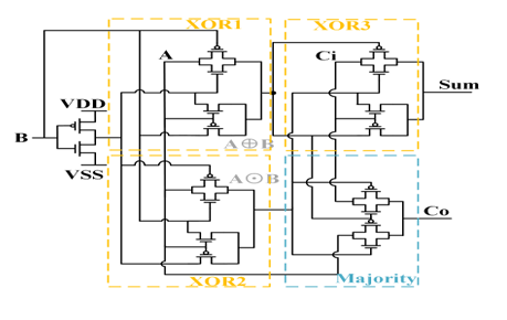
Block Diagram
Specifications
· Tool Used: Cadence EDA tools for schematic and simulation
· Design Elements: complementary compound push–pull pair (PMOS + NMOS), input matching network, L1 & L2 (0.5 pH–10 pH) inductors, high-value output load (RL, 100 kΩ–1 MΩ), biasing/level-shift network, feedback/compensation path, input/output coupling and decoupling capacitors, thermal-stabilization circuitry, and symmetric/layout considerations for reduced mismatch
· Optimization Goal: minimize circuit complexity and parasitics (transistor and passive count) while preserving ultra-wideband large-signal gain, low output noise, high temperature stability, and linearity across the desired cutoff range (e.g., maintain cutoff from ≈18.21 kHz up to hundreds of GHz in simulation) with low power consumption (~69 mW)v
Learning Outcomes
· Understanding the working principle of Pass Transistor Logic (PTL)
· Ability to design a low-power full adder using PTL techniques
· Knowledge of SUM and CARRY generation using reduced transistor count
· Ability to analyze power, delay, and area trade-offs in PTL-based designs
· Experience in optimizing transistor-level topology
· Familiarity with transistor-level schematic design of PTL full adders
· Hands-on exposure to simulation and waveform analysis of PTL circuits
· Understanding of low-voltage and energy-efficient arithmetic circuit design
Demo Video


Request for Video
Related Projects
 Paper Publishing
Request Call Back
Would you like to receive a free callback now?
Choose the best time for callback:
Leave your message and we will contact you as soon as possible

6-2-85/B, Old Maternity Hospital Road, Thyagaraja Nagar, Tirupati, Andhra Pradesh – 517501
+91 9030333433
+91 9393939065
0877-2261612

Disclaimer - Takeoff Edu Group Projects are not associated or affiliated with IEEE in any way. The IEEE Projects mentioned here are mentioned in the context of student projects, whose ideas are derived from IEEE publications, not projects of or by IEEE.