Implementation of 32Bit Carry LookAhead Adder using PTL logic
Objective
High-speed arithmetic units are essential for modern digital systems, where addition plays a critical role in overall processor performance. The Carry Look-Ahead Adder (CLA) is widely used due to its ability to reduce carry propagation delay by generating carry signals in parallel. This work presents the implementation of a 32-bit Carry Look-Ahead Adder using Pass Transistor Logic (PTL) to achieve improved speed and reduced power consumption. PTL logic minimizes transistor count by efficiently utilizing pass transistors for logic realization, leading to lower switching activity and reduced silicon area compared to conventional CMOS logic
Abstract
High-speed arithmetic units are essential for modern digital systems, where addition plays a critical role in overall processor performance. The Carry Look-Ahead Adder (CLA) is widely used due to its ability to reduce carry propagation delay by generating carry signals in parallel. This work presents the implementation of a 32-bit Carry Look-Ahead Adder using Pass Transistor Logic (PTL) to achieve improved speed and reduced power consumption. PTL logic minimizes transistor count by efficiently utilizing pass transistors for logic realization, leading to lower switching activity and reduced silicon area compared to conventional CMOS logic. The proposed 32-bit CLA architecture employs propagate and generate signals to compute carry outputs hierarchically, thereby eliminating sequential carry dependency. The design is implemented and simulated using CMOS technology, and the results demonstrate that the PTL-based CLA offers enhanced performance in terms of delay and power efficiency, making it suitable for high-performance and low-power VLSI applications.
Keywords: Carry Look-Ahead Adder (CLA), Pass Transistor Logic (PTL), 32-bit Adder, High-Speed Arithmetic Circuits, Low-Power VLSI Design, CMOS Technology, Carry Propagation Reduction.NOTE: Without the concern of our team, please don't submit to the college. This Abstract varies based on student requirements.
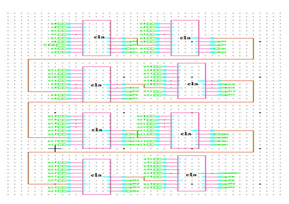
Block Diagram
Specifications
· Tool Used: Tanner EDA tools for schematic and simulation
· Technology Node: 45nm CMOS process.
· Counter Width: 7-bit
· Design Elements: AND,XOR,RCA, FA,
· Optimization Goal: The primary optimization goal of this project is to reduce the overall transistor count while maintaining accurate arithmetic operation in the 32-bit Carry Look-Ahead Adder implemented using Pass Transistor Logic (PTL). By employing PTL-based gate structures and hierarchical carry look-ahead computation, the design minimizes redundant logic and switching activity, leading to lower area and power consumption. At the same time, correct logical functionality is preserved across all operating conditions, ensuring reliable carry generation and sum computation without functional errors or signal degradation. This optimized approach achieves an efficient balance between hardware complexity and performance, making the design suitable for low-power and high-speed VLSI applications.
Learning Outcomes
- Understand the working principle and architecture of Carry Look-Ahead Adders (CLA).
- Gain practicalSS knowledge of Pass Transistor Logic (PTL) and its advantages over conventional CMOS logic.
- Learn hierarchical design techniques for implementing large bit-width arithmetic circuits.
- Develop skills in transistor-level schematic design and optimization for low power and area.
- Analyze carry propagation, delay, and power consumption in high-speed adders.
- Acquire experience in using EDA tools for schematic entry, simulation, and verification.
- Understand the impact of technology scaling and transistor sizing on circuit performance.
- Improve ability to debug and resolve simulation errors related to device modeling and sizing.
Demo Video


Request for Video
Related Projects
 Paper Publishing
Request Call Back
Would you like to receive a free callback now?
Choose the best time for callback:
Leave your message and we will contact you as soon as possible

6-2-85/B, Old Maternity Hospital Road, Thyagaraja Nagar, Tirupati, Andhra Pradesh – 517501
+91 9030333433
+91 9393939065
0877-2261612

Disclaimer - Takeoff Edu Group Projects are not associated or affiliated with IEEE in any way. The IEEE Projects mentioned here are mentioned in the context of student projects, whose ideas are derived from IEEE publications, not projects of or by IEEE.