Hybrid Logical Effort for Hybrid Logic Style Full Adders in Multistage Structures
Also Available Domains Cadence EDA|Tanner EDA
Objective
This paper proposes an efficient analysis and modeling technique that enables designers to assess the timing behavior of hybrid full adder circuits at the block level and anticipate their performance in multistage circuits.
Abstract
One of the critical issues in the advancement of very large scale of integration circuit design is the estimation of timing behavior of the arithmetic circuits. The concept of logical effort provides a proficient approach to comprehend and assess the timing behavior of circuits with conventional CMOS (C-CMOS) structure. However, this technique is not working for circuits with a hybrid structure. On the other hand, numerous circuits with the hybrid structure which are faster and consume less power than C-CMOS one have been proposed for different applications such as portable and IoT devices. In this regard, the necessity of having and use of a simple and efficient timing behavior method like conventional logical effort for analysis of the hybrid adder circuits is inevitable. This paper proposes an efficient analysis and modeling technique that enables designers to assess the timing behavior of hybrid full adder circuits at the block level and anticipate their performance in multistage circuits. The gain and selection factor are introduced as a criterion for accurate selection and optimization of the hybrid adder cells measurable on the single test bench for management of energy efficiency and performance tradeoff. The proposed method is investigated using 32-nm CMOS and FinFET technologies.
NOTE: Without the concern of our team, please don't submit to the college. This Abstract varies based on student requirements.
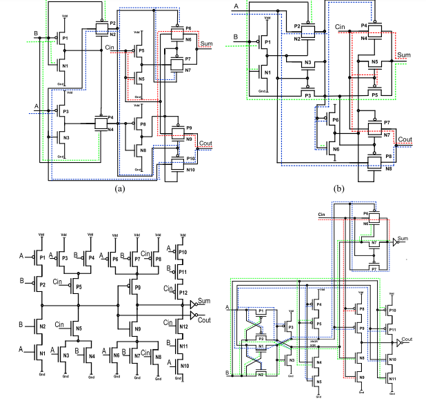
Block Diagram
Specifications

Contact Us
- info@takeoffprojects.com
- +91 9030333433, +91 9393939065


 Paper Publishing

Request Call Back
Would you like to receive a free callback now?
Choose the best time for callback:
Leave your message and we will contact you as soon as possible

6-2-85/B, Old Maternity Hospital Road, Thyagaraja Nagar, Tirupati, Andhra Pradesh – 517501
+91 9030333433
+91 9393939065
0877-2261612

Disclaimer - Takeoff Edu Group Projects are not associated or affiliated with IEEE in any way. The IEEE Projects mentioned here are mentioned in the context of student projects, whose ideas are derived from IEEE publications, not projects of or by IEEE.