High-Precision Hybrid CMOS MTJ BGR With Improved Temperature Coefficient and Reduced Area
Objective
The increasing demand for low-power analog and mixed-signal systems has created a need for compact and flexible reference voltage generator circuits capable of providing multiple programmable voltage levels.
Abstract
The increasing demand for precision analog and mixed-signal integrated circuits has accelerated the development of highly accurate and area-efficient Bandgap Reference (BGR) circuits with excellent temperature stability. Conventional CMOS bandgap reference circuits often suffer from large silicon area, higher temperature coefficients, process-induced variations, and limited long-term stability. This work presents a High-Precision Hybrid CMOS/Magnetic Tunnel Junction (MTJ) Bandgap Reference (BGR) with an improved temperature coefficient and reduced silicon area. The proposed architecture combines a conventional CMOS bandgap reference with MTJ-based resistive elements to achieve superior reference voltage stability while minimizing the circuit footprint. The design incorporates a precision operational amplifier, proportional-to-absolute-temperature (PTAT) current generator, complementary-to-absolute-temperature (CTAT) voltage generator, MTJ-based resistor network, and current mirror circuits to improve temperature compensation and process robustness. The proposed BGR is evaluated in terms of reference voltage accuracy, temperature coefficient, line regulation, power consumption, process-voltage-temperature (PVT) variations, silicon area, and long-term stability. Simulation results demonstrate a significantly improved temperature coefficient, enhanced reference voltage accuracy, reduced silicon area, and lower power consumption compared with conventional CMOS-only bandgap reference architectures. The proposed Hybrid CMOS/MTJ BGR provides a reliable, compact, and energy-efficient voltage reference solution for precision analog, mixed-signal, automotive, industrial, and IoT applications.
NOTE: Without the concern of our team, please don't submit to the college. This Abstract varies based on student requirements.
Block Diagram
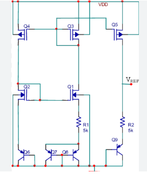
Specifications
· Tool Used: Cadence EDA tools for schematic and simulation
· Technology Node:45nm CMOS process.
· Design Elements: Precision voltage reference core, CMOS resistor network, current mirrors, voltage selection switches, low-power buffer amplifier, startup circuit, bias current generator, and compensation circuitry.
Optimization Goal: Minimize power consumption, silicon area, line regulation error, load regulation error, settling time, and temperature coefficient while maximizing reference voltage accuracy, output voltage programmability, stability, and overall circuit efficiencyLearning Outcomes
· Understand the operating principles of CMOS reference voltage generator circuits.
· Learn the architecture of multiple and variable reference voltage generators.
· Study current mirror and resistor network design techniques.
· Analyze line regulation and load regulation performance.
· Evaluate power consumption and temperature stability.
· Understand programmable voltage selection methods.
· Design and simulate a low-power variable reference voltage generator using Cadence Virtuoso CMOS tools.


 Paper Publishing

Request Call Back
Would you like to receive a free callback now?
Choose the best time for callback:
Leave your message and we will contact you as soon as possible

6-2-85/B, Old Maternity Hospital Road, Thyagaraja Nagar, Tirupati, Andhra Pradesh – 517501
+91 9030333433
+91 9393939065
0877-2261612

Disclaimer - Takeoff Edu Group Projects are not associated or affiliated with IEEE in any way. The IEEE Projects mentioned here are mentioned in the context of student projects, whose ideas are derived from IEEE publications, not projects of or by IEEE.