High-Linearity CMOS VCO for FMCW Radar
Objective
This work presents the design and implementation of a high-linearity CMOS Voltage-Controlled Oscillator (VCO) for Frequency-Modulated Continuous Wave (FMCW) radar applications. FMCW radar systems require highly linear frequency modulation to ensure accurate distance and velocity estimation. However, conventional CMOS VCOs suffer from nonlinearity in frequency tuning, phase noise, and limited tuning range, which degrade radar performance
Abstract
This work presents the design and implementation of a high-linearity CMOS Voltage-Controlled Oscillator (VCO) for Frequency-Modulated Continuous Wave (FMCW) radar applications. FMCW radar systems require highly linear frequency modulation to ensure accurate distance and velocity estimation. However, conventional CMOS VCOs suffer from nonlinearity in frequency tuning, phase noise, and limited tuning range, which degrade radar performance.
In this design, a high-linearity VCO architecture is developed using optimized varactor tuning, current control techniques, and improved biasing methods to achieve a linear frequency-voltage relationship. The proposed VCO is implemented in CMOS technology and analyzed for key performance parameters such as tuning range, linearity, phase noise, and power consumption. The design focuses on minimizing frequency deviation errors and improving spectral purity.
Simulation results demonstrate that the proposed VCO achieves enhanced linearity, reduced phase noise, and stable operation across the desired frequency range, making it highly suitable for FMCW radar systems used in automotive, industrial, and sensing applications.
Keywords
CMOS VCO, FMCW Radar, High Linearity, Phase Noise, Frequency Tuning, Low Power, RF Design
NOTE: Without the concern of our team, please don't submit to the college. This Abstract varies based on student requirements.
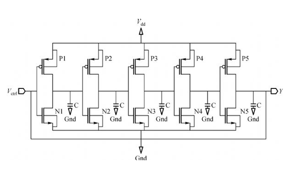
Block Diagram
Specifications
· Tool Used: Cadence EDA tools for schematic and simulation
· Technology Node:180nm CMOS process.
· Design Elements: complementary compound push–pull pair (PMOS + NMOS), input matching network, L1 & L2 (0.5 pH–10 pH) inductors, high-value output load (RL, 100 kΩ–1 MΩ), biasing/level-shift network, feedback/compensation path, input/output coupling and decoupling capacitors, thermal-stabilization circuitry, and symmetric/layout considerations for reduced mismatch
· Optimization Goal: minimize circuit complexity and parasitics (transistor and passive count) while preserving ultra-wideband large-signal gain, low output noise, high temperature stability, and linearity across the desired cutoff range (e.g., maintain cutoff from ≈18.21 kHz up to hundreds of GHz in simulation) with low power consumption (~69 mW)v
Learning Outcomes
Understanding of VCO Design Principles
• Knowledge of FMCW Radar Requirements
• Analysis of Frequency Linearity and Phase Noise
• RF Circuit Design Techniques in CMOS
• Performance Optimization in Oscillators
• Hands-on Experience with RF Simulation Tools


 Paper Publishing

Request Call Back
Would you like to receive a free callback now?
Choose the best time for callback:
Leave your message and we will contact you as soon as possible

6-2-85/B, Old Maternity Hospital Road, Thyagaraja Nagar, Tirupati, Andhra Pradesh – 517501
+91 9030333433
+91 9393939065
0877-2261612

Disclaimer - Takeoff Edu Group Projects are not associated or affiliated with IEEE in any way. The IEEE Projects mentioned here are mentioned in the context of student projects, whose ideas are derived from IEEE publications, not projects of or by IEEE.