FPGA implementation of high speed vedic multiplier
Also Available Domains Arithmetic Core|Xilinx Vivado
Abstract
Multiplication is an operation much needed in Digital Signal Processing for various applications. This paper puts forward a high speed Vedic multiplier which is efficient in terms of speed, making use of Urdhva Tiryagbhyam, a sutra from Vedic Math for multiplication and Kogge Stone algorithm for performing addition of partial products and also compares it with the characteristics of existing algorithms. The below two algorithms aids to parallel generation of partial products and faster carry generation respectively, leading to better performance. The code is written in Verilog HDL and implemented on Artix 7 using Xilinx vivado
Index Terms— Vedic Multiplication, real-time processing
NOTE: Without the concern of our team, please don't submit to the college. This Abstract varies based on student requirements.
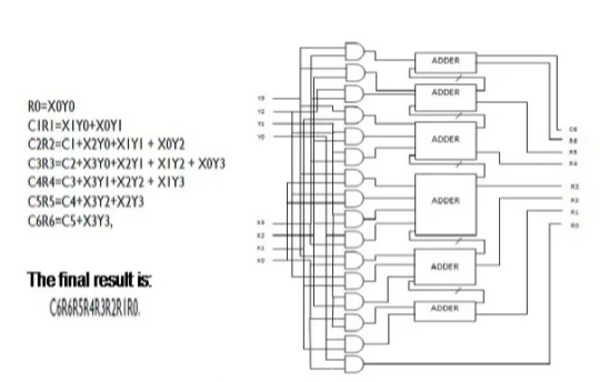
Block Diagram
Specifications
System Configuration:-
In the hardware part a normal computer where Xilinx ISE 14.3 software can be easily operated is required, i.e., with a minimum system configuration
Hardware requirement
Processor - Pentium –III
Speed - 1.1 GHz
RAM - 1 GB (min)
Hard Disk - 40 GB
Floppy Drive - 1.44 MB
Key Board - Standard Windows Keyboard
Mouse - Two or Three Button Mouse
Monitor - SVGA
Software requirements
v Operating System :Windows95/98/2000/XP/Windows7
v Front End : Modelsim 6.3 for Debugging and Xilinx 14.3 for Synthesis and Hard Ware Implementation
v This software’s where Verilog source code can be used for design implementation.
Learning Outcomes
Understanding of Vedic multiplication: Students will gain a deep understanding of Vedic multiplication techniques and their advantages over conventional multiplication methods. They will learn how to break down multiplication into smaller, more manageable steps using Vedic sutras.
Knowledge of FPGA architecture: Students will become familiar with the architecture and functionality of Field Programmable Gate Arrays (FPGAs). They will learn how to leverage the flexibility and reconfigurability of FPGAs to implement complex arithmetic operations efficiently.
FPGA design flow: Students will learn the entire FPGA design flow, including designing the Vedic multiplier using a Hardware Description Language (HDL) such as Verilog or VHDL, simulating the design, synthesizing it to a target FPGA device, and programming the FPGA.
Efficient implementation techniques: Students will explore various techniques to optimize the Vedic multiplier design for speed, area, or power consumption, depending on the specific design goals. This may include pipelining, parallelization, resource sharing, and other optimization strategies.
Performance evaluation and analysis: Students will learn how to evaluate the performance of their implemented Vedic multiplier on the FPGA, considering metrics such as throughput, latency, and resource utilization. They will analyze the results to identify potential bottlenecks and areas for improvement.
Troubleshooting and debugging: As with any hardware implementation, students will encounter challenges and issues during the FPGA design process. They will develop skills in troubleshooting and debugging their designs, identifying and resolving problems that may arise.
Documentation and presentation skills: Students will gain experience in documenting their design process, including writing clear and concise design specifications, test plans, and implementation reports. They will also develop presentation skills to effectively communicate their work and findings to an audience.
Collaboration and teamwork: If this project is conducted as a group assignment or in a collaborative setting, students will learn how to work together effectively, distribute tasks, and integrate individual contributions into a cohesive FPGA implementation.


 Paper Publishing

Request Call Back
Would you like to receive a free callback now?
Choose the best time for callback:
Leave your message and we will contact you as soon as possible

6-2-85/B, Old Maternity Hospital Road, Thyagaraja Nagar, Tirupati, Andhra Pradesh – 517501
+91 9030333433
+91 9393939065
0877-2261612

Disclaimer - Takeoff Edu Group Projects are not associated or affiliated with IEEE in any way. The IEEE Projects mentioned here are mentioned in the context of student projects, whose ideas are derived from IEEE publications, not projects of or by IEEE.