Design & Verification of AMBA AHB-Lite Memory Controller
Objective
The main aim of this project is to implement AMBA-3AHB lite to perform read/write operations
Abstract
As technology advances, the on-chip communication bus architecture becomes increasingly prominent in interconnecting various components within the System-on-Chip (SoC). The standard ARM AMBA on-chip interconnect bus is designed as an SoC system’s high-performance backbone bus, which supports faster communication with internal and external memories. This paper presented a memory controller design with an AMBA 3 AHB Lite standard based on a single master and multiple slave model.
NOTE: Without the concern of our team, please don't submit to the college. This Abstract varies based on student requirements.
Block Diagram
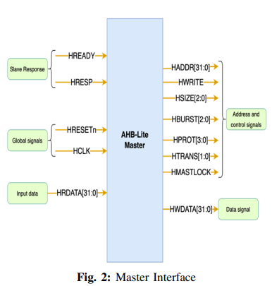
Specifications
Software Requirements:
· Xilinx ISE14.7 Suite/Vivado2018.3 Tool.
· HDL: Verilog.
Hardware Requirements:
· Microsoft® Windows XP.
· Intel® Pentium® 4 processor or Pentium 4 equivalent with SSE support.
· 512 MB RAM.
· 100 MB of available disk space.
Learning Outcomes
• Basics of Digital Electronics
• FPGA design Flow
• Introduction to Verilog Coding
• Different modeling styles in Verilog
o Data Flow modeling
o Structural modeling
o Behavioral modeling
o Mixed level modeling
• Drawbacks of existing methods
• Applications in real time
• Xilinx ISE 14.7/Xilinx Vivado for design and simulation
• Generation of Netlist
• Solution providing for real time problems
• Project Development Skills:
o Problem Analysis Skills
o Problem Solving Skills
o Logical Skills
o Designing Skills
o Testing Skills.
o Debugging Skills.
o Presentation Skills.
o Thesis Writing Skills
Demo Video


Request for Video
 Paper Publishing
Request Call Back
Would you like to receive a free callback now?
Choose the best time for callback:
Leave your message and we will contact you as soon as possible

6-2-85/B, Old Maternity Hospital Road, Thyagaraja Nagar, Tirupati, Andhra Pradesh – 517501
+91 9030333433
+91 9393939065
0877-2261612

Disclaimer - Takeoff Edu Group Projects are not associated or affiliated with IEEE in any way. The IEEE Projects mentioned here are mentioned in the context of student projects, whose ideas are derived from IEEE publications, not projects of or by IEEE.