Design of Two Stage Operational Amplifier and Implementation of Flash ADC
Also Available Domains Transistor Logic|Cadence EDA|Tanner EDA
Objective
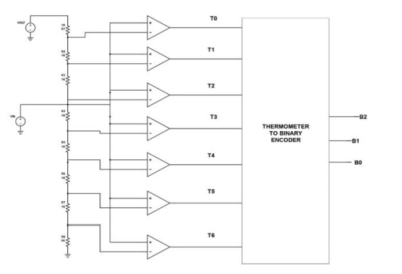
The aim of this paper is to implement a Flash ADC structure consists of a resistive ladder network, comparators, and the thermometer to a binary encoder. Encoder structure in this paper is implemented using 2:1 mux based on switch logic.
Abstract
In this paper, Flash Analog to digital converter is implemented whose resolution is 3-bits.The major problem that usually appears in flash ADC is as the number of resolution bits increases, the Area, as well as the power consumption of the circuit, also increases. It is preferred to have digital systems that are portable and have prolonged battery life. This can be only possible by developing applications that consume less power. In this paper, we principally concentrated to lessen the power consumption of the ADC by optimizing encoder circuitry. The entire design is implemented using Tanner EDA\Cadence Virtuoso tools employing 180nm technology. Performance parameters of Flash ADC such as delay as well as average power are calculated and compared.
NOTE: Without the concern of our team, please don't submit to the college. This Abstract varies based on student requirements.
Block Diagram

Specifications
Software Requirements:
- Tanner EDA\Cadence Virtuoso
- Technology files: 180nm
Hardware Requirements:
- Microsoft® Windows XP
- Intel® Pentium® 4 processor or Pentium 4 equivalent with SSE support
- 512 MB RAM
- 100 MB of available disk space
Learning Outcomes
- Introduction to ADC
- Types of ADC
- Limitations & Applications.
- Introduction to Op-amp
- Knowledge on two stage op-amp
- Applications
- Introduction to encoders
- Knowledge of designing encoder using various logics
- Encoder using full adder
- Encoder using mux
- Importance of Transistors
- MOS Fundamentals
- NMOS/PMOS/CMOS Technologies
- How to design circuits using Transistor logic?
- Transistor level design for op-amp & encoder
- How to design Flash ADC using two stage op-amp & encoder.
- Introduction to Analog Electronics
- Importance of Two stage Op-amp & switch Logic
- Scope of Switch logic in today’s world
- Applications in Real time.
- Tanner EDA\Cadence Virtuoso tool for design and simulation
- Solution providing for real time problems
- Project Development Skills:
- Problem Analysis Skills
- Problem Solving Skills
- Logical Skills
- Designing Skills
- Testing Skills
- Debugging Skills
- Presentation skills
- Thesis Writing Skills


 Paper Publishing
