Design of Start up Enabled Bandgap Voltage Reference
Objective
The project presents the design and implementation of a start-up enabled Bandgap Voltage Reference (BGR) circuit using 180 nm technology, aimed at providing a stable and temperature-independent reference voltage for analog and mixed-signal VLSI systems. The proposed BGR generates a reference voltage of 1.20?V across a wide temperature range of -40?°C to 140?°C, with a low temperature coefficient of 12.71?ppm/°C, while consuming only 72.6?µW of power.
Abstract
The project presents the design and implementation of a start-up enabled Bandgap Voltage Reference (BGR) circuit using 180 nm technology, aimed at providing a stable and temperature-independent reference voltage for analog and mixed-signal VLSI systems. The proposed BGR generates a reference voltage of 1.20 V across a wide temperature range of -40 °C to 140 °C, with a low temperature coefficient of 12.71 ppm/°C, while consuming only 72.6 µW of power. The design integrates both CTAT (Complementary to Absolute Temperature) and PTAT (Proportional to Absolute Temperature) voltage generation using MOSFETs and BJTs, and employs a start-up circuit to ensure reliable operation during power-on transients. Pre-layout and post-layout simulations using the Sky130 PDK show close agreement, validating the circuit’s performance against supply voltage variations and transient conditions. The proposed BGR offers a compact, low-power, and high-precision voltage reference suitable for applications in ADCs, DACs, memory circuits, PLLs, and other analog and mixed-signal systems.
KEYWORDS: Bandgap Reference, CMOS, Complementary to Absolute Temperature (CTAT), Proportional to Absolute Temperature (PTAT), Voltage Reference, Temperature
NOTE: Without the concern of our team, please don't submit to the college. This Abstract varies based on student requirements.
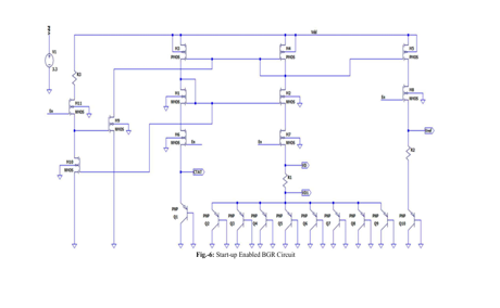
Block Diagram
Specifications
· Tool Used: Cadence EDA tools for schematic and simulation
· Technology Node:180nm CMOS process.
· Design Elements: complementary compound push–pull pair (PMOS + NMOS), input matching network, L1 & L2 (0.5 pH–10 pH) inductors, high-value output load (RL, 100 kΩ–1 MΩ), biasing/level-shift network, feedback/compensation path, input/output coupling and decoupling capacitors, thermal-stabilization circuitry, and symmetric/layout considerations for reduced mismatch
· Optimization Goal: minimize circuit complexity and parasitics (transistor and passive count) while preserving ultra-wideband large-signal gain, low output noise, high temperature stability, and linearity across the desired cutoff range (e.g., maintain cutoff from ≈18.21 kHz up to hundreds of GHz in simulation) with low power consumption (~69 mW)v
Learning Outcomes
· Understand the principles of Bandgap Reference (BGR) circuits, including CTAT and PTAT voltage generation.
· Learn how to design temperature-independent voltage references for analog and mixed-signal VLSI systems.
· Gain knowledge of start-up circuits to ensure proper operation during power-on transients.
· Analyze the effects of temperature and supply voltage variations on circuit performance.
· Develop skills in pre-layout and post-layout simulations using Sky130 PDK.
· Compare design trade-offs such as power consumption, accuracy, and temperature range in BGR designs.
· Apply theoretical concepts practically by designing circuits using MOSFETs and BJTs.
Demo Video


Request for Video
 Paper Publishing
Request Call Back
Would you like to receive a free callback now?
Choose the best time for callback:
Leave your message and we will contact you as soon as possible

6-2-85/B, Old Maternity Hospital Road, Thyagaraja Nagar, Tirupati, Andhra Pradesh – 517501
+91 9030333433
+91 9393939065
0877-2261612

Disclaimer - Takeoff Edu Group Projects are not associated or affiliated with IEEE in any way. The IEEE Projects mentioned here are mentioned in the context of student projects, whose ideas are derived from IEEE publications, not projects of or by IEEE.