DESIGN OF SPI AND I2C PROTOCOL IN VERILOG HDL
Objective
This paper introduces the structure and working principle of SPI communication bus, analyzes its timing structure and four working modes, and uses this state machine method to realize its SPI bus communication function & also this paper focuses on the design of I2C single master which consists of a bidirectional data line i.e. serial data line (sda) and serial clock line (scl).
Abstract
The SPI bus is a synchronous serial interface data bus with full duplex, few signal lines, simple protocol, and fast transmission speed. Based on these characteristics, parallel high-speed computing with FPGA is used to meet device expansion and experiment in high-rate environments. This paper introduces the structure and working principle of SPI communication bus, analyzes its timing structure and four working modes, and uses this state machine method to realize its SPI bus communication function & also this paper focuses on the design of I2C single master which consists of a bidirectional data line i.e. serial data line (sda) and serial clock line (scl). This protocol has the ability to support multiple masters. I2C is a two-wire, bidirectional serial bus that provides a simple and efficient method of data exchange between devices and is used for faster devices to communicate with slower devices and each other without data loss. It requires only two lines for communication with two or more chips and can control a network of device chips with just two general purpose I/O pins whereas, other bus protocols require more pins and signals to connect devices. The module circuit of SPI & I2C is written by Verilog hardware description language, and the waveform is simulated in vivado simulator. After the simulation waveform analysis, the feasibility of the state machine method is verified.
NOTE: Without the concern of our team, please don't submit to the college. This Abstract varies based on student requirements.
Block Diagram
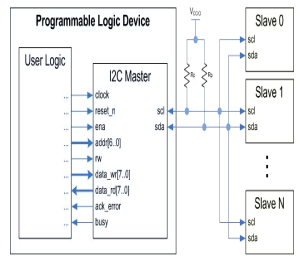
Specifications
Software Requirements:
· Xilinx Vivado Tool
· HDL: Verilog
Learning Outcomes
Learning Outcomes:
- Basics of Digital Electronics
- VLSI design Flow
- Introduction to Verilog Coding
- Different modeling styles in Verilog
o Data Flow modeling
o Structural modeling
o Behavioral modeling
o Mixed level modeling
- Introduction to protocols
- About I2C protocol
- Knowledge master & slave
- Knowledge on FSM
- About SPI protocol
- Applications in real time
· Xilinx ISE 14.7/Xilinx Vivado for design and simulation
· Generation of Netlist
· Solution providing for real time problems
· Project Development Skills:
o Problem Analysis Skills
o Problem Solving Skills
o Logical Skills
o Designing Skills
o Testing Skills
o Debugging Skills
o Presentation Skills
o Thesis Writing Skills


Related Projects
 Paper Publishing

Request Call Back
Would you like to receive a free callback now?
Choose the best time for callback:
Leave your message and we will contact you as soon as possible

6-2-85/B, Old Maternity Hospital Road, Thyagaraja Nagar, Tirupati, Andhra Pradesh – 517501
+91 9030333433
+91 9393939065
0877-2261612

Disclaimer - Takeoff Edu Group Projects are not associated or affiliated with IEEE in any way. The IEEE Projects mentioned here are mentioned in the context of student projects, whose ideas are derived from IEEE publications, not projects of or by IEEE.