Design of Full Adder and Parity Generator Based on Reversible Logic
Objective
The main objective of this project is to design a full adder and parity generator using reversible logic gates in order to reduce power dissipation.
Abstract
In this project, a full adder and a parity generator circuit is presented using the proposed reversible logic gate in QCA technology. As stated in the Moore’s law the transistor level should get double in every two years, researches is being carried out to find different technology to replace VLSI. QCA technology is the standout among and giving a better solution because it is a nano-technology. It provides high speed, low power consumption and higher density as compared to CMOS technology. The reversible logic gates in QCA are useful in reducing energy dissipation. Here in the proposed work a novel design for reversible logic gate is proposed which can be used as a full adder, even or odd parity generator as well. The proposed circuit is simple in structure to construct and it doesn’t produce any garbage value too. We have used very less number of clock cycles or zones while making this circuit and also it is suitable for implementing other logical gates. The whole project is implemented and verified by simulating it in QCA Designer & QCA DesignerE tools.
Keywords: full adder, parity generator, reversible logic gate, QCA technology, Moore’s law, VLSI, nano technology, energy dissipation, QCA Designer, QCA DesignerE.
NOTE: Without the concern of our team, please don't submit to the college. This Abstract varies based on student requirements.
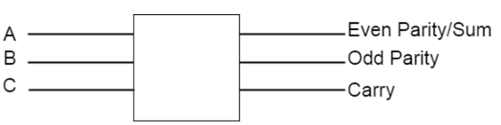
Block Diagram
Specifications
Specifications:
Software Requirements:
· QCA Designer
· QCA DesignerE
Hardware Requirements:
· Microsoft® Windows XP
· Intel® Pentium® 4 processor or Pentium 4 equivalent with SSE support
· 512 MB RAM
· 100 MB of available disk space
Learning Outcomes
Learning Outcomes:
- Introduction to Nano-technology
- Knowledge on Quantum Dot cellular automata
- Digital Circuit Fundamentals
- Introduction to reversible logic gates
- How to design circuits using QCA Designer
- Quantum cell level design for digital circuits
- Learn to design high speed, area efficient QCA circuits
- Importance of clock cycles in QCA technology
- Techniques for reducing energy dissipation
- Scope of reversible circuits in quantum computing
- Applications in real time
- QCA Designer and QCA designerE tool for design and simulation
- Solution providing for real time problems
· Project Development Skills:
o Problem Analysis Skills
o Problem Solving Skills
o Logical Skills
o Designing Skills
o Testing Skills
o Debugging Skills
o Presentation Skills
o Thesis Writing Skills


Related Projects
 Paper Publishing

Request Call Back
Would you like to receive a free callback now?
Choose the best time for callback:
Leave your message and we will contact you as soon as possible

6-2-85/B, Old Maternity Hospital Road, Thyagaraja Nagar, Tirupati, Andhra Pradesh – 517501
+91 9030333433
+91 9393939065
0877-2261612

Disclaimer - Takeoff Edu Group Projects are not associated or affiliated with IEEE in any way. The IEEE Projects mentioned here are mentioned in the context of student projects, whose ideas are derived from IEEE publications, not projects of or by IEEE.