Design of a Scalable Low-Power 1-bit Hybrid Full Adder for Fast Computation
Also Available Domains Low Power VLSI|Tanner EDA
Abstract
This work presents the design of a scalable low-power 1-bit hybrid full adder optimized for fast computation in modern digital systems. The proposed architecture combines the advantages of conventional CMOS logic with hybrid design techniques to achieve a balance between speed, power, and area efficiency. By carefully selecting logic styles and minimizing transistor count, the design significantly reduces switching activity and short-circuit power dissipation while maintaining robust logic functionality. The adder is implemented using advanced CMOS technology and evaluated for key performance parameters including propagation delay, power consumption, power-delay product (PDP), and scalability to higher-bit arithmetic circuits. Simulation results demonstrate that the hybrid adder achieves lower delay and reduced power compared to traditional full adder implementations, making it highly suitable for applications in portable devices, low-power processors, and high-speed arithmetic logic units. The proposed design also ensures scalability, enabling its integration into larger arithmetic modules such as multipliers and ALUs without significant performance degradation. This research contributes to the development of energy-efficient arithmetic circuits for next-generation VLSI systems.
Keywords
• Hybrid Full Adder
• Low Power Design
• High-Speed Computation
• CMOS Logic
• Scalable Arithmetic Circuits
• Propagation Delay
• Power-Delay Product (PDP)
• VLSI Design
• Arithmetic Logic Unit (ALU)
• Energy-Efficient Digital Circuits
NOTE: Without the concern of our team, please don't submit to the college. This Abstract varies based on student requirements.
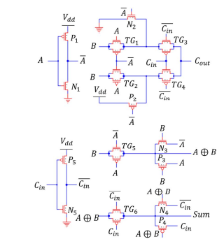
Block Diagram
Specifications
Software Requirements:
• Tool: Cadence
Hardware Requirements:
• Microsoft® Windows XP
• Intel® Pentium® 4 processor or Pentium 4 equivalent with SSE support
• 512 MB RAM
• 100 MB of available disk space
Learning Outcomes
-
Understanding the principles of hybrid full adder design combining CMOS and alternative logic styles.
-
Ability to implement low-power, high-speed arithmetic circuits using Cadence Virtuoso and Spectre simulation tools.
-
Knowledge of transistor-level design optimization for reducing propagation delay and power consumption.
-
Practical skills in schematic design, layout creation, and parasitic extraction in Cadence tools.
-
Experience in evaluating performance metrics such as power-delay product (PDP), area, and speed.
-
Understanding the trade-offs between speed, power, and area in full adder and arithmetic circuit design.
-
Competence in scaling 1-bit adder design to multi-bit adders for integration into ALUs and processors.
-
Familiarity with advanced CMOS technology nodes (65 nm, 45 nm, 32 nm) for energy-efficient circuit design.
-
Ability to perform simulation-based verification and optimization of arithmetic circuits.
-
Preparedness to apply low-power, high-speed design techniques in VLSI and embedded system applications.


 Paper Publishing

Request Call Back
Would you like to receive a free callback now?
Choose the best time for callback:
Leave your message and we will contact you as soon as possible

6-2-85/B, Old Maternity Hospital Road, Thyagaraja Nagar, Tirupati, Andhra Pradesh – 517501
+91 9030333433
+91 9393939065
0877-2261612

Disclaimer - Takeoff Edu Group Projects are not associated or affiliated with IEEE in any way. The IEEE Projects mentioned here are mentioned in the context of student projects, whose ideas are derived from IEEE publications, not projects of or by IEEE.