Design of 8 bit Arithmetic Logic Unit for Signal Processing Applications using Verilog
Objective
The objective of this project is to design and implement an 8-bit Arithmetic Logic Unit (ALU) using Verilog for efficient signal processing applications. It focuses on performing various arithmetic and logical operations with high speed and accuracy. The design will be simulated and verified to ensure correct functionality and optimized performance in digital computation. Special attention is given to minimizing delay and power consumption while maintaining design flexibility. The overall goal is to develop a reliable and high-performance ALU suitable for integration into signal processing and embedded system architectures.
Abstract
Abstract:
This work built an 8-bit arithmetic logic unit. The arithmetic logic unit is the fundamental building block of every signal processing operation. ALU is designed for performing 16 operations including addition, subtraction, multiplication, logical, bitwise, shifting, increment and decrement. Three inputs, four select lines are given to ALU as inputs and output is obtained. This ALU is implemented in Vivado 2024 software using Verilog language and FPGA target device selected is xc7a100tcsg324-1. Two methods are used to implement ALU. ALU is implemented using behavioral and structural level modelling style. Synthesis results of both the methods are calculated.NOTE: Without the concern of our team, please don't submit to the college. This Abstract varies based on student requirements.
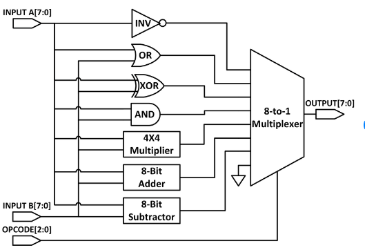
Block Diagram
Specifications
Software Requirements:
· Xilinx ISE14.7 Suite/Vivado2018.3 Tool.
· HDL: Verilog.
Hardware Requirements:
· Microsoft® Windows XP.
· Intel® Pentium® 4 processor or Pentium 4 equivalent with SSE support.
· 512 MB RAM.
· 100 MB of available disk space.
Learning Outcomes
Understand the architecture and operation of an 8-bit ALU
· Design ALU using behavioral and structural Verilog modeling
· Implement multiple arithmetic and logical operations in hardware
· Analyze synthesis results such as area and delay
· Compare modeling styles in FPGA-based digital design
· Gain practical experience using Vivado and FPGA targets


Related Projects
 Paper Publishing

Request Call Back
Would you like to receive a free callback now?
Choose the best time for callback:
Leave your message and we will contact you as soon as possible

6-2-85/B, Old Maternity Hospital Road, Thyagaraja Nagar, Tirupati, Andhra Pradesh – 517501
+91 9030333433
+91 9393939065
0877-2261612

Disclaimer - Takeoff Edu Group Projects are not associated or affiliated with IEEE in any way. The IEEE Projects mentioned here are mentioned in the context of student projects, whose ideas are derived from IEEE publications, not projects of or by IEEE.