Design and Study the Performance of a CMOS-Based Ring Oscillator Architecture for 5G Mobile Communication
Also Available Domains Cadence EDA|Low Power VLSI
Objective
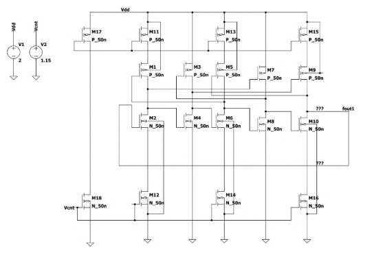
CMOS-Based Ring Oscillator Design The primary goal is to design a ring oscillator architecture using complementary metal-oxide-semiconductor (CMOS) technology. This choice of technology is crucial for 5G applications due to its scalability and low power consumption.
Abstract
Oscillator circuits generate precise and reliable clock signals, essential for applications ranging from simple wristwatches to complex satellite systems, particularly in long-distance communication. These circuits can be built using either passive or active components, each with its own advantages and drawbacks. In the current era of mobile communication, the emphasis is on interoperability and low power consumption, driving the need for compact, battery-powered electronics. VLSI-based ring oscillators have emerged as an ideal solution due to their power efficiency, compactness, and wide tuning range. This paper presents a novel CMOS ring oscillator designed to function as a Voltage Controlled Oscillator (VCO). The proposed architecture combines the benefits of a current-starved ring oscillator and a negative-skewed delay, achieving optimized control and supply voltages while producing a dominant frequency with minimal harmonic distortion. By carefully selecting passive components, this design is well-suited for 5G applications that require high frequency and low power consumption.
Key words: - VLSI; 5G; CMOS; Ring Oscillator; VCO; Mobile Communication.
NOTE: Without the concern of our team, please don't submit to the college. This Abstract varies based on student requirements.
Block Diagram
Specifications
Software Requirements:
- Tool: Cadence Virtuoso
- Technology: GPDK 45nm
Hardware Requirements:
- Microsoft® Windows XP
- Intel® Pentium® 4 processor or Pentium 4 equivalent with SSE support
- 512 MB RAM
- 100 MB of available disk space
Learning Outcomes
· Introduction to Analog & Digital Electronics
· Advantages & Applications of Oscillator.
· Basics of VCO
o Different configurations of VCO
· Knowledge on Ring Oscillator
· Design of oscillator in Cadence
· Analysis of simulation results & Outputs
· Scope of oscillator in today’s world.
· Real time applications of oscillator.


Related Projects
 Paper Publishing

Request Call Back
Would you like to receive a free callback now?
Choose the best time for callback:
Leave your message and we will contact you as soon as possible

6-2-85/B, Old Maternity Hospital Road, Thyagaraja Nagar, Tirupati, Andhra Pradesh – 517501
+91 9030333433
+91 9393939065
0877-2261612

Disclaimer - Takeoff Edu Group Projects are not associated or affiliated with IEEE in any way. The IEEE Projects mentioned here are mentioned in the context of student projects, whose ideas are derived from IEEE publications, not projects of or by IEEE.