Design and Implementation of RNB multiplier Using NP Domino logic
Objective
The main objective of this project is to reduce the delay of RNB multiplier using NP Domino Logic.
Abstract
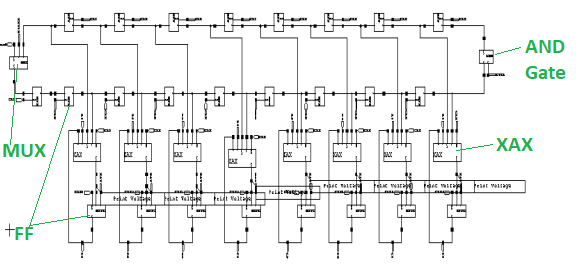
In this paper, a Reordered Normal Basis (RNB) finite field multiplier is implemented using NP domino logic. This multiplier uses RNB, which is the type-II Optimal Normal Basis (ONB), to perform multiplication. The Critical Path Delay (CPD) is influenced by the XOR-AND-XOR (XAX) module of the Serial-In Parallel-Out (SIPO) RNB multiplier. Hence, this block is designed in NP domino logic. The Tanner EDA 32nm tool is used to design the multiplier using the full-custom design. The major goal is to determine the optimum logic style that meets the VLSI optimization requirements like the area, multiplication delay, CPD, power dissipation, Area-Delay Product (APD), and Power-Delay Product (PDP). When compared to other logic styles, the delay and area of the multiplier employing NP domino logic are lower, whereas the power dissipation is similar to other domino logic styles.
NOTE: Without the concern of our team, please don't submit to the college. This Abstract varies based on student requirements.
Block Diagram
Specifications
Specifications:
Software Requirements:
l Tanner EDA
l Technology: 32nm
Hardware Requirements:
l Microsoft® Windows XP
l Intel® Pentium® 4 processor or Pentium 4 equivalent with SSE support
l 512 MB RAM
l 100 MB of available disk space
Learning Outcomes
l Introduction to Finite Fields
l Knowledge on different basis in Galois Field [GF]
l Overview of RNB Multiplier
l Basics of Flip-flops & its Applications
l Knowledge on Different types of Shift Registers
l Fundamentals of MOSFETs
l Learning of different configurations in CMOS
l Software learning of Tanner EDA in terms of designing & simulating.
l Scope of RNB multiplier in today’s world.
Demo Video


Request for Video
 Paper Publishing
Request Call Back
Would you like to receive a free callback now?
Choose the best time for callback:
Leave your message and we will contact you as soon as possible

6-2-85/B, Old Maternity Hospital Road, Thyagaraja Nagar, Tirupati, Andhra Pradesh – 517501
+91 9030333433
+91 9393939065
0877-2261612

Disclaimer - Takeoff Edu Group Projects are not associated or affiliated with IEEE in any way. The IEEE Projects mentioned here are mentioned in the context of student projects, whose ideas are derived from IEEE publications, not projects of or by IEEE.