Design and Implementation of a 4-Bit Carry Save Adder Using MTCMOS-Based Ripple Carry Adder with 10T Full Adders in 90nm Technology
Objective
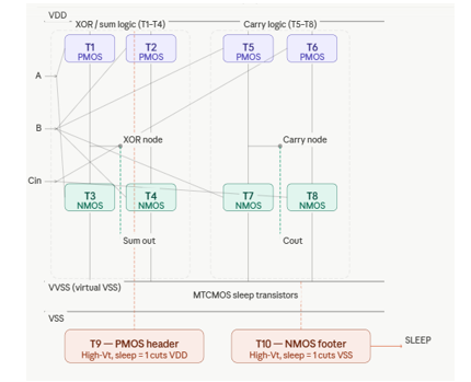
This work presents the design and implementation of a 4-bit Carry Save Adder (CSA) utilizing a Multi-Threshold CMOS (MTCMOS)-based Ripple Carry Adder (RCA) constructed with 10-transistor (10T) full adders in 90nm technology. With the increasing demand for high-speed and low-power arithmetic circuits in digital systems, efficient adder architectures play a crucial role in enhancing overall system performance
Abstract
This work presents the design and implementation of a 4-bit Carry Save Adder (CSA) utilizing a Multi-Threshold CMOS (MTCMOS)-based Ripple Carry Adder (RCA) constructed with 10-transistor (10T) full adders in 90nm technology. With the increasing demand for high-speed and low-power arithmetic circuits in digital systems, efficient adder architectures play a crucial role in enhancing overall system performance. The carry save adder is widely used to reduce propagation delay in multi-operand addition by eliminating immediate carry propagation.
In the proposed design, MTCMOS technique is employed to minimize leakage power by using high-threshold transistors as sleep devices, effectively reducing standby power consumption. The 10T full adder cells are optimized to achieve a balance between reduced transistor count, power efficiency, and speed. By integrating CSA with an MTCMOS-based RCA, the design achieves fast intermediate computation and efficient final carry propagation. The circuit is implemented and simulated in 90nm CMOS technology, and its performance is evaluated in terms of power consumption, delay, and power-delay product (PDP). Results demonstrate significant improvements in energy efficiency and speed compared to conventional CMOS adder designs, making it suitable for low-power and high-performance VLSI applications.
Keywords
Carry Save Adder, MTCMOS, Ripple Carry Adder, 10T Full Adder, Low Power, 90nm CMOS, VLSI Design
NOTE: Without the concern of our team, please don't submit to the college. This Abstract varies based on student requirements.
Block Diagram
Specifications
· Tool Used: Cadence EDA tools for schematic and simulation
· Technology Node:180nm CMOS process.
· Design Elements: complementary compound push–pull pair (PMOS + NMOS), input matching network, L1 & L2 (0.5 pH–10 pH) inductors, high-value output load (RL, 100 kΩ–1 MΩ), biasing/level-shift network, feedback/compensation path, input/output coupling and decoupling capacitors, thermal-stabilization circuitry, and symmetric/layout considerations for reduced mismatch
· Optimization Goal: minimize circuit complexity and parasitics (transistor and passive count) while preserving ultra-wideband large-signal gain, low output noise, high temperature stability, and linearity across the desired cutoff range (e.g., maintain cutoff from ≈18.21 kHz up to hundreds of GHz in simulation) with low power consumption (~69 mW)v
Learning Outcomes
• Understanding of Carry Save Adder Architecture
• Knowledge of Ripple Carry Adder Design
• Application of MTCMOS Technique for Leakage Reduction
• Design of Low-Transistor Full Adders (10T)
• Performance Analysis Using Power, Delay, and PDP
• Hands-on Experience with VLSI Design Tools


 Paper Publishing

Request Call Back
Would you like to receive a free callback now?
Choose the best time for callback:
Leave your message and we will contact you as soon as possible

6-2-85/B, Old Maternity Hospital Road, Thyagaraja Nagar, Tirupati, Andhra Pradesh – 517501
+91 9030333433
+91 9393939065
0877-2261612

Disclaimer - Takeoff Edu Group Projects are not associated or affiliated with IEEE in any way. The IEEE Projects mentioned here are mentioned in the context of student projects, whose ideas are derived from IEEE publications, not projects of or by IEEE.