Design and implementation of 16 Bit SAR ADC for high resolution
Also Available Domains Low Power VLSI|Transistor Logic
Objective
Build a high-resolution SAR ADC capable of 16-bit accuracy by leveraging advanced calibration, low-noise comparator and CDAC design, and optimized architecture (segmented CDAC, redundancy, efficient SAR logic), all while maintaining practical speed, low power, and manufacturable silicon performance.
Abstract
NOTE: Without the concern of our team, please don't submit to the college. This Abstract varies based on student requirements.
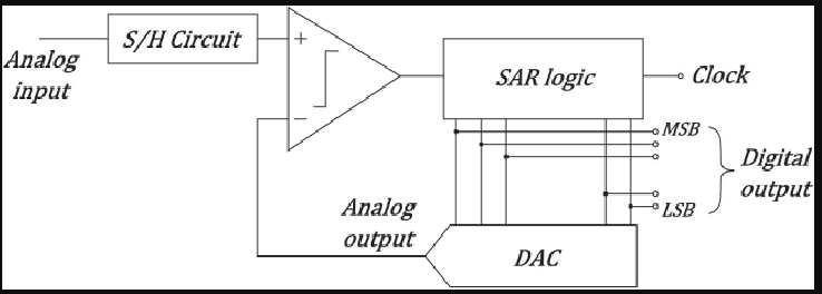
Block Diagram
Specifications
Software Requirements:
• Tool: Cadence
Hardware Requirements:
• Microsoft® Windows XP
• Intel® Pentium® 4 processor or Pentium 4 equivalent with SSE support
• 512 MB RAM
• 100 MB of available disk space
Learning Outcomes
1.Understanding self-timed circuit design: Gain knowledge about the concept of self-timed or asynchronous circuit design. Learn about the advantages and challenges of self-timed circuits compared to synchronous designs, including improved performance, reduced power consumption, and increased robustness against timing variations.
2.Familiarity with parallel adder architecture: Explore the architecture and operation of parallel adders. Understand how parallel adders perform addition operations on multiple bits simultaneously, enabling faster computation and higher throughput.
3.Knowledge of transmission gate logic: Learn about transmission gate logic and its suitability for implementing digital circuits. Understand the characteristics, advantages, and limitations of transmission gate logic, including low propagation delay, low power consumption, and bidirectional signal handling.
4.Understanding the adder components: Gain insights into the key components of a parallel adder, such as the carry propagation stage and sum calculation stage. Understand their functions, dependencies, and interconnections in achieving accurate addition results.
5.Analyzing self-timed circuit behavior: Explore the behavior of self-timed circuits, including the concept of handshaking protocols, delay-insensitive design, and timing independence. Understand how self-timed circuits achieve correct operation regardless of varying delays or signal arrival times.
6.Designing a parallel self-timed adder: Apply the knowledge gained to design a parallel self-timed adder using transmission gate logic style. Understand the design considerations, such as circuit topology, interconnectivity, and timing constraints, to ensure correct and efficient operation.
7.Simulation and analysis: Utilize simulation tools and techniques to validate the designed self-timed adder. Analyze its performance in terms of speed, power consumption, and robustness against timing variations. Gain hands-on experience in simulating and evaluating self-timed circuits to verify their functionality.
8.Evaluating trade-offs: Develop the ability to evaluate trade-offs between speed, power consumption, area utilization, and other performance metrics in self-timed adder design. Understand how design choices, such as the sizing of transmission gates and circuit topology, impact these trade-offs and make informed decisions based on the specific requirements of the adder.
9.Documentation and reporting: Develop effective communication skills by documenting the design process, results, and findings in a clear and concise manner. Prepare a comprehensive report summarizing the design, implementation, and performance analysis of the parallel self-timed adder using transmission gate logic style.
10.Critical thinking and problem-solving: Enhance critical thinking and problem-solving skills by identifying and addressing challenges and limitations in the design process. Explore alternative design techniques, optimization strategies, and circuit modifications to improve the adder's performance and address potential issues.
Demo Video


Request for Video
Related Projects
 Paper Publishing
Request Call Back
Would you like to receive a free callback now?
Choose the best time for callback:
Leave your message and we will contact you as soon as possible

6-2-85/B, Old Maternity Hospital Road, Thyagaraja Nagar, Tirupati, Andhra Pradesh – 517501
+91 9030333433
+91 9393939065
0877-2261612

Disclaimer - Takeoff Edu Group Projects are not associated or affiliated with IEEE in any way. The IEEE Projects mentioned here are mentioned in the context of student projects, whose ideas are derived from IEEE publications, not projects of or by IEEE.