Design and analysis of hybrid 10T adder for low power applications
Objective
This study presents a novel 10-transistor (10T) hybrid full adder architecture designed for ultra-low power applications using 45nm CMOS process technology. The design employs an energy-efficient hybrid logic multiplexer approach incorporating Gate Diffusion Input (GDI) logic, aiming to reduce both power consumption and chip area while maintaining performance. The proposed architecture features level restoration carry logic that ensures full swing output voltage, addressing the voltage degradation issues commonly found in conventional 10T adder designs
Abstract
This study presents a novel 10-transistor (10T) hybrid full adder architecture designed for ultra-low power applications using 45nm CMOS process technology. The design employs an energy-efficient hybrid logic multiplexer approach incorporating Gate Diffusion Input (GDI) logic, aiming to reduce both power consumption and chip area while maintaining performance. The proposed architecture features level restoration carry logic that ensures full swing output voltage, addressing the voltage degradation issues commonly found in conventional 10T adder designs. Comprehensive simulations were conducted using Mentor Graphics tools at various supply voltages (0.8V and 1.2V), and the results demonstrate significant improvements over existing full adder designs, including a 65% reduction in transistor count compared to traditional CMOS logic adders and a 37% reduction compared to transmission gate adders. The proposed design achieves at least 80% enhancement in power-delay product (PDP) parameters when compared to existing architectures, with the level restoration technique-based version consuming 13% less power and exhibiting 90% less delay than the version without level restoration, making it highly suitable for resource-constrained, energy-efficient digital systems.
KEYWORDS: Hybrid full adder , 10T adder , Low power design, CMOS technology, Gate Diffusion Input (GDI) logic , Level restoration technique , Ultra-low voltage (ULV).
NOTE: Without the concern of our team, please don't submit to the college. This Abstract varies based on student requirements.
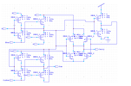
Block Diagram
Specifications
· Tool Used: Tanner EDA tools for schematic and simulation
· Technology Node: 250 CMOS process.
· Counter Width: 7-bit
· Design Elements: TFF(D), RCA, FA, and DFF with clip logic.
· Optimization Goal: Reduce transistor count while ensuring accurate up/down counting with clipping at terminal values.
Learning Outcomes
1. Understanding of Low Power VLSI Design Techniques
2. Knowledge of Hybrid Logic Design Approaches
3. Familiarity with Gate Diffusion Input (GDI) Logic
4. Comprehension of Full Adder Circuit Architectures
5. Understanding of Level Restoration Techniques
6. Knowledge of Threshold Voltage Degradation Issues
7. Proficiency in Multiplexer-Based Circuit Design
Demo Video


Request for Video
Related Projects
 Paper Publishing
Request Call Back
Would you like to receive a free callback now?
Choose the best time for callback:
Leave your message and we will contact you as soon as possible

6-2-85/B, Old Maternity Hospital Road, Thyagaraja Nagar, Tirupati, Andhra Pradesh – 517501
+91 9030333433
+91 9393939065
0877-2261612

Disclaimer - Takeoff Edu Group Projects are not associated or affiliated with IEEE in any way. The IEEE Projects mentioned here are mentioned in the context of student projects, whose ideas are derived from IEEE publications, not projects of or by IEEE.