Constructing DNA Full Adder Circuit Based on the Simple and Efficient AND Logic Blocks
Objective
This work presents the design and implementation of a DNA-based full adder circuit constructed using simple and efficient AND logic blocks. With the growing demand for alternative computing paradigms beyond conventional CMOS technology, DNA computing has emerged as a promising approach due to its inherent parallelism, low power consumption, and high data storage capability
Abstract
This work presents the design and implementation of a DNA-based full adder circuit constructed using simple and efficient AND logic blocks. With the growing demand for alternative computing paradigms beyond conventional CMOS technology, DNA computing has emerged as a promising approach due to its inherent parallelism, low power consumption, and high data storage capability. In the proposed design, basic logic operations are realized through DNA strand displacement and hybridization processes, where AND logic blocks act as the fundamental building units. The full adder circuit is developed by integrating these AND-based modules with complementary logic structures to generate accurate sum and carry outputs. The proposed architecture focuses on reducing reaction complexity, minimizing the number of DNA strands, and improving computational reliability. Simulation and theoretical analysis demonstrate enhanced efficiency, lower error rates, and reduced biochemical reactions compared to existing DNA-based logic circuits. This design is highly suitable for applications in molecular computing, bio-sensing systems, and nano-scale information processing.
Keywords
DNA Computing, Full Adder, AND Logic Block, Strand Displacement, Molecular Logic Circuits, Bio-Computing, Nanoelectronics
NOTE: Without the concern of our team, please don't submit to the college. This Abstract varies based on student requirements.
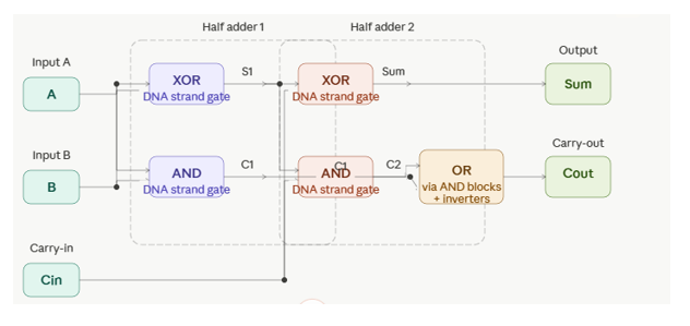
Block Diagram
Specifications
· Tool Used: Cadence EDA tools for schematic and simulation
· Technology Node:180nm CMOS process.
· Design Elements: complementary compound push–pull pair (PMOS + NMOS), input matching network, L1 & L2 (0.5 pH–10 pH) inductors, high-value output load (RL, 100 kΩ–1 MΩ), biasing/level-shift network, feedback/compensation path, input/output coupling and decoupling capacitors, thermal-stabilization circuitry, and symmetric/layout considerations for reduced mismatch
· Optimization Goal: minimize circuit complexity and parasitics (transistor and passive count) while preserving ultra-wideband large-signal gain, low output noise, high temperature stability, and linearity across the desired cutoff range (e.g., maintain cutoff from ≈18.21 kHz up to hundreds of GHz in simulation) with low power consumption (~69 mW)v
Learning Outcomes
Understanding of DNA Computing Principles
• Design of Molecular Logic Circuits
• Implementation of Full Adder Using Biochemical Reactions
• Knowledge of Strand Displacement Mechanism
• Analysis of Reaction Efficiency and Error Reduction
• Exposure to Nano-Scale Computing Technologies


Related Projects
 Paper Publishing

Request Call Back
Would you like to receive a free callback now?
Choose the best time for callback:
Leave your message and we will contact you as soon as possible

6-2-85/B, Old Maternity Hospital Road, Thyagaraja Nagar, Tirupati, Andhra Pradesh – 517501
+91 9030333433
+91 9393939065
0877-2261612

Disclaimer - Takeoff Edu Group Projects are not associated or affiliated with IEEE in any way. The IEEE Projects mentioned here are mentioned in the context of student projects, whose ideas are derived from IEEE publications, not projects of or by IEEE.