Area-Efficient and Low-Power 8T Compute-SRAM Bitcell Design for Digital Compute-In-Memory Macros in 22nm CMOS
Objective
This work presents the design of an area-efficient and low-power 8-transistor (8T) Compute-SRAM bitcell tailored for digital compute-in-memory (CIM) macros in 22nm CMOS technology. With the rapid growth of data-intensive applications such as artificial intelligence, machine learning, and edge computing, conventional von Neumann architectures face significant limitations due to excessive data movement between memory and processing units
Abstract
This work presents the design of an area-efficient and low-power 8-transistor (8T) Compute-SRAM bitcell tailored for digital compute-in-memory (CIM) macros in 22nm CMOS technology. With the rapid growth of data-intensive applications such as artificial intelligence, machine learning, and edge computing, conventional von Neumann architectures face significant limitations due to excessive data movement between memory and processing units. Compute-in-memory (CIM) has emerged as a promising solution to overcome this bottleneck by enabling computation directly within memory arrays.
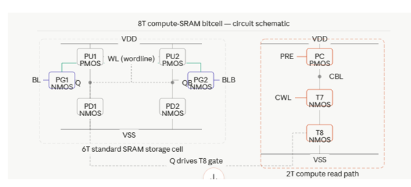
In this design, an optimized 8T SRAM bitcell is developed to support both reliable data storage and in-memory logic operations. The proposed bitcell separates read and write paths to enhance stability and reduce read disturbance, while additional transistors enable efficient computation within the memory array. The design focuses on minimizing area overhead and reducing power consumption through optimized transistor sizing and reduced switching activity. Implemented in 22nm CMOS technology, the proposed bitcell demonstrates improved energy efficiency, reduced delay, and enhanced robustness compared to conventional 6T SRAM cells and existing CIM designs. This makes it highly suitable for next-generation low-power, high-performance digital compute-in-memory systems.
Keywords
Compute-In-Memory, 8T SRAM, Low Power, Area Efficient, 22nm CMOS, Digital CIM, Memory Bitcell Design
NOTE: Without the concern of our team, please don't submit to the college. This Abstract varies based on student requirements.
Block Diagram
Specifications
· Tool Used: Cadence EDA tools for schematic and simulation
· Technology Node:180nm CMOS process.
· Design Elements: complementary compound push–pull pair (PMOS + NMOS), input matching network, L1 & L2 (0.5 pH–10 pH) inductors, high-value output load (RL, 100 kΩ–1 MΩ), biasing/level-shift network, feedback/compensation path, input/output coupling and decoupling capacitors, thermal-stabilization circuitry, and symmetric/layout considerations for reduced mismatch
· Optimization Goal: minimize circuit complexity and parasitics (transistor and passive count) while preserving ultra-wideband large-signal gain, low output noise, high temperature stability, and linearity across the desired cutoff range (e.g., maintain cutoff from ≈18.21 kHz up to hundreds of GHz in simulation) with low power consumption (~69 mW)v
Learning Outcomes
• Understanding of SRAM Bitcell Architectures (6T vs 8T)
• Knowledge of Compute-In-Memory Concepts
• Low-Power VLSI Design Techniques
• Stability Analysis of SRAM Cells
• Performance Evaluation Using PDP and Noise Margins
• Exposure to Advanced CMOS Technology (22nm)
Demo Video


Request for Video
 Paper Publishing
Request Call Back
Would you like to receive a free callback now?
Choose the best time for callback:
Leave your message and we will contact you as soon as possible

6-2-85/B, Old Maternity Hospital Road, Thyagaraja Nagar, Tirupati, Andhra Pradesh – 517501
+91 9030333433
+91 9393939065
0877-2261612

Disclaimer - Takeoff Edu Group Projects are not associated or affiliated with IEEE in any way. The IEEE Projects mentioned here are mentioned in the context of student projects, whose ideas are derived from IEEE publications, not projects of or by IEEE.