An Asymmetric Dynamic Comparator for Low Offset, Low Noise, and High Speed Applications
Objective
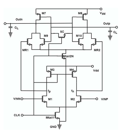
This project presents the design and analysis of a charge-shared two-tail dynamic latch comparator intended for low-power and high-speed Successive Approximation Register Analog-to-Digital Converter (SAR-ADC) applications. With the growing demand for energy-efficient portable and biomedical electronic systems, reducing comparator power consumption without compromising speed and accuracy has become critical. In this work, Fig. 3 is newly designed based on an existing comparator architecture by incorporating a shared charge technique between the output nodes, which effectively reduces power dissipation and regeneration delay
Abstract
This project presents the design and analysis of a charge-shared two-tail dynamic latch comparator intended for low-power and high-speed Successive Approximation Register Analog-to-Digital Converter (SAR-ADC) applications. With the growing demand for energy-efficient portable and biomedical electronic systems, reducing comparator power consumption without compromising speed and accuracy has become critical. In this work, Fig. 3 is newly designed based on an existing comparator architecture by incorporating a shared charge technique between the output nodes, which effectively reduces power dissipation and regeneration delay. The proposed comparator operates on a dynamic latch principle with dual tail transistors and an additional charge-sharing transistor that stabilizes the output nodes during the reset phase. The design is implemented and simulated using CMOS technology, and its performance is evaluated in terms of delay, power consumption, and power-delay product (PDP). Simulation results demonstrate that the proposed design achieves significant improvements in energy efficiency and speed compared to conventional dynamic comparators, making it highly suitable for low-power SAR-ADC architectures used in biomedical, communication, and portable electronic applications.
KEYWORDS: Successive Approximation Register-ADC, Low power, High speed, Sampling rate, Resolution, Electronic devicesNOTE: Without the concern of our team, please don't submit to the college. This Abstract varies based on student requirements.
Block Diagram
Specifications
· Tool Used: Cadence EDA tools for schematic and simulation
· Technology Node:180nm CMOS process.
· Design Elements: complementary compound push–pull pair (PMOS + NMOS), input matching network, L1 & L2 (0.5 pH–10 pH) inductors, high-value output load (RL, 100 kΩ–1 MΩ), biasing/level-shift network, feedback/compensation path, input/output coupling and decoupling capacitors, thermal-stabilization circuitry, and symmetric/layout considerations for reduced mismatch
· Optimization Goal: minimize circuit complexity and parasitics (transistor and passive count) while preserving ultra-wideband large-signal gain, low output noise, high temperature stability, and linearity across the desired cutoff range (e.g., maintain cutoff from ≈18.21 kHz up to hundreds of GHz in simulation) with low power consumption (~69 mW)v
Learning Outcomes
· Understanding of SAR-ADC Architecture
· Design of Dynamic Latch Comparators
· Application of Charge Sharing Techniques
· Low-Power CMOS Circuit Design Skills
· Performance Analysis Using Delay and PDP
· Simulation and Validation Using CAD Tools
Demo Video


Request for Video
Related Projects
 Paper Publishing
Request Call Back
Would you like to receive a free callback now?
Choose the best time for callback:
Leave your message and we will contact you as soon as possible

6-2-85/B, Old Maternity Hospital Road, Thyagaraja Nagar, Tirupati, Andhra Pradesh – 517501
+91 9030333433
+91 9393939065
0877-2261612

Disclaimer - Takeoff Edu Group Projects are not associated or affiliated with IEEE in any way. The IEEE Projects mentioned here are mentioned in the context of student projects, whose ideas are derived from IEEE publications, not projects of or by IEEE.