A Wideband Input Buffer Based on Cascade Complementary Source Follower
Also Available Domains Cadence EDA
Objective
Wideband Operation – Designing an input buffer that can handle a broad frequency range with minimal signal distortion
Abstract
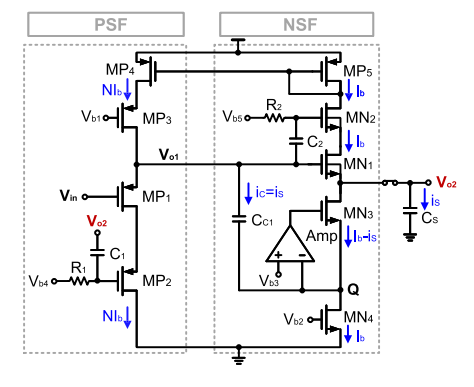
A highly linear input buffer is essential for high-speed, high-resolution analog-to-digital converters (ADCs) as it effectively isolates kickback noise and package inductance. This brief analyzes several key factors influencing input buffer linearity and introduces a wideband, high-linearity input buffer based on a cascaded complementary source follower (CCSF) architecture. The proposed CCSF input buffer combines a pMOS source follower (PSF) and an nMOS source follower (NSF).
To enhance bandwidth and minimize distortion, it incorporates a compensation capacitor, an assisted operational amplifier (opamp), a bootstrapped-capacitor level-shifting circuit, a current amplifier, and various optimization techniques. The design was simulated and verified using the Cadence 45nm technology software tool, affirming its effectiveness and practicality.
Keywords: Input buffer, linearization, sample and hold circuit, source follower, wideband.
NOTE: Without the concern of our team, please don't submit to the college. This Abstract varies based on student requirements.
Block Diagram
Specifications
Software Requirements:
• Tool: Cadence virtuoso
• Technology: 45nm
Learning Outcomes
• Basics of Digital Electronics
• Logic Gates
• Op-amp
• Introduction to Cadence virtuoso
• Buffer importance
• Rea time applications
Project Development Skills:
o Problem Analysis Skills
o Problem Solving Skills
o Logical Skills
o Designing Skills


 Paper Publishing

Request Call Back
Would you like to receive a free callback now?
Choose the best time for callback:
Leave your message and we will contact you as soon as possible

6-2-85/B, Old Maternity Hospital Road, Thyagaraja Nagar, Tirupati, Andhra Pradesh – 517501
+91 9030333433
+91 9393939065
0877-2261612

Disclaimer - Takeoff Edu Group Projects are not associated or affiliated with IEEE in any way. The IEEE Projects mentioned here are mentioned in the context of student projects, whose ideas are derived from IEEE publications, not projects of or by IEEE.