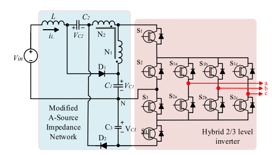
A Three-Level Single Stage A-Source Inverter with the Ability to Generate Active Voltage Vector during Shoot-Through State
Objective
The main objective of this project is to gain the capability for applying an active voltage vector during the shoot-through state.
Abstract
In this paper, as the boosting stage for a three-level inverter, a new modified configuration of A-source IN with two series outputs is proposed and connected to a 10-switches three-level inverter. Besides generating two outputs by a single IN, the proposed DC/AC inverter is able to apply an active voltage vector during the ST state. This capability improves the DC/AC voltage gain, increases the modulation index, and decreases the required ST time. The operation principles are described, and the steady-state relations are derived. It is compared with other magnetically coupled INs in terms of boost factor and voltage stress of switches. Considering the 10-switches three-level inverter as the front-end inverter, an adopted maximum boost strategy using the space vector modulation is developed targeting minimum ST time. The performance of the proposed topology is validated through the MATLAB-based simulations.
Keywords: Impedance source network, A-Source impedance network, multi-level inverter, maximum boost space vector, PWM.
NOTE: Without the concern of our team, please don't submit to the college. This Abstract varies based on student requirements.
Block Diagram

Specifications
Software Configuration:
Operating System : Windows 7/8/10
Application Software : Matlab/Simulink
Hardware Configuration:
RAM : 8 GB
Processor : I3 / I5(Mostly prefer)
Learning Outcomes
- Introduction to Matlab/Simulink
- What is EISPACK & LINPACK
- How to start with MATLAB
- About Matlab language
- About tools & libraries
- Application of Matlab/Simulink
- About Matlab desktop
- Features of Matlab/Simulink
- Basics on Matlab/Simulink
- Introduction to controllers.
- Study of PWM techniques.
- Project Development Skills:
- Problem analyzing skills
- Problem solving skills
- Creativity and imaginary skills
- Programming skills
- Deployment
- Testing skills
- Debugging skills
- Project presentation skills
- Thesis writing skills


 Paper Publishing
