A Static, Contention-Free, Low-Power, TSPC Dual-Edge Triggered Flip-Flop
Objective
This work presents the design and implementation of a static, contention-free, low-power True Single-Phase Clock (TSPC) dual-edge triggered flip-flop (DETFF) for high-performance and energy-efficient digital systems. Flip-flops are fundamental building blocks in synchronous circuits, and their power consumption significantly impacts overall system efficiency. Conventional single-edge triggered flip-flops require higher clock frequencies to achieve desired throughput, leading to increased dynamic power consumption
Abstract
This work presents the design and implementation of a static, contention-free, low-power True Single-Phase Clock (TSPC) dual-edge triggered flip-flop (DETFF) for high-performance and energy-efficient digital systems. Flip-flops are fundamental building blocks in synchronous circuits, and their power consumption significantly impacts overall system efficiency. Conventional single-edge triggered flip-flops require higher clock frequencies to achieve desired throughput, leading to increased dynamic power consumption.
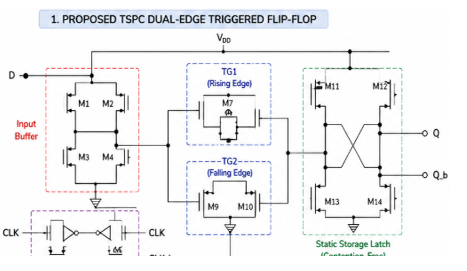
The proposed design utilizes a dual-edge triggering mechanism, allowing data to be captured on both rising and falling edges of the clock signal, effectively reducing clock frequency requirements by half. The TSPC technique enables single-phase clock operation, simplifying clock distribution and reducing clock power. Additionally, the contention-free architecture eliminates short-circuit current paths during switching, thereby reducing power dissipation.
The flip-flop is implemented using CMOS technology and evaluated in terms of power consumption, delay, and power-delay product (PDP). Simulation results demonstrate reduced power consumption, improved efficiency, and reliable operation compared to conventional flip-flop designs, making it suitable for low-power, high-speed applications.
Keywords
TSPC Flip-Flop, Dual-Edge Triggered Flip-Flop, Low Power, Contention-Free, CMOS, Sequential Circuits, VLSI Design
NOTE: Without the concern of our team, please don't submit to the college. This Abstract varies based on student requirements.
Block Diagram
Specifications
· Tool Used: Cadence EDA tools for schematic and simulation
· Technology Node:180nm CMOS process.
· Design Elements: complementary compound push–pull pair (PMOS + NMOS), input matching network, L1 & L2 (0.5 pH–10 pH) inductors, high-value output load (RL, 100 kΩ–1 MΩ), biasing/level-shift network, feedback/compensation path, input/output coupling and decoupling capacitors, thermal-stabilization circuitry, and symmetric/layout considerations for reduced mismatch
· Optimization Goal: minimize circuit complexity and parasitics (transistor and passive count) while preserving ultra-wideband large-signal gain, low output noise, high temperature stability, and linearity across the desired cutoff range (e.g., maintain cutoff from ≈18.21 kHz up to hundreds of GHz in simulation) with low power consumption (~69 mW)v
Learning Outcomes
• Understanding of Dual-Edge Triggered Flip-Flops
• Knowledge of TSPC Design Technique
• Low-Power Sequential Circuit Design
• Contention Reduction Techniques
• Performance Analysis Using PDP
• Experience with CMOS Circuit Simulation


Related Projects
 Paper Publishing

Request Call Back
Would you like to receive a free callback now?
Choose the best time for callback:
Leave your message and we will contact you as soon as possible

6-2-85/B, Old Maternity Hospital Road, Thyagaraja Nagar, Tirupati, Andhra Pradesh – 517501
+91 9030333433
+91 9393939065
0877-2261612

Disclaimer - Takeoff Edu Group Projects are not associated or affiliated with IEEE in any way. The IEEE Projects mentioned here are mentioned in the context of student projects, whose ideas are derived from IEEE publications, not projects of or by IEEE.