A Novel Technique to Improve Performance Evaluation of Domino Logic Circuits in CMOS and FinFET Technology
Also Available Domains Low Power VLSI|Cadence EDA
Objective
In this paper, a high-speed and Ultra-Low power FinFET technology-based domino OR circuit is discussed with various OR domino logic are simulated in the MOS and FinFET (SG & LP modes) technologies
Abstract
In this project, a Low Power Stacked (LPS) FinFET based Domino logic for the 8 input OR gate is proposed. As the silicon industries miniaturizing the device size and increasing the performance day by day to implement more functionality in digital ICs, we elaborate a different technique which is used to design domino logic circuits. Power consumption can be minimized without deteriorating the performance of the circuit and the efficiency of the circuit can be increases with proposed technique.
With low power characteristics and great performance improvement in FinFET devices changes are obtained in higher ION/IOFF ratio and the leakage current is reduced and it fastens the switching speed. All the designs are implemented using 180nm technology in Cadence Virtuoso.
Keywords: CMOS, FinFET, Low Power, Domino.
NOTE: Without the concern of our team, please don't submit to the college. This Abstract varies based on student requirements.
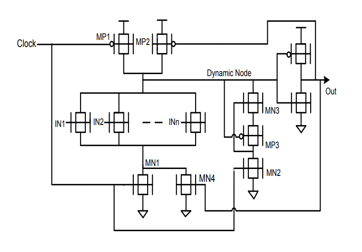
Block Diagram
Specifications
Software Requirements:
- Cadence Virtuoso
- Technology files:180nm
Hardware Requirements:
- Microsoft® Windows XP
- Intel® Pentium® 4 processor or Pentium 4 equivalent with SSE support
- 512 MB RAM
- 100 MB of available disk space


 Paper Publishing

Request Call Back
Would you like to receive a free callback now?
Choose the best time for callback:
Leave your message and we will contact you as soon as possible

6-2-85/B, Old Maternity Hospital Road, Thyagaraja Nagar, Tirupati, Andhra Pradesh – 517501
+91 9030333433
+91 9393939065
0877-2261612

Disclaimer - Takeoff Edu Group Projects are not associated or affiliated with IEEE in any way. The IEEE Projects mentioned here are mentioned in the context of student projects, whose ideas are derived from IEEE publications, not projects of or by IEEE.