A Novel Energy Efficient 4-Bit Vedic Multiplier Using Modified GDI Approach at 32 nm Technology
Objective
This paper proposes a novel energy-efficient 4-bit Vedic multiplier designed using a modified Gate Diffusion Input (GDI) technique implemented at 32 nm CMOS technology. Vedic mathematics, derived from ancient Indian scriptures, provides highly efficient algorithms for arithmetic operations. The Urdhva Tiryagbhyam sutra of Vedic mathematics is employed here as the core multiplication algorithm due to its inherent parallelism, which reduces the number of computational steps and minimizes partial product generation delay
Abstract
This paper proposes a novel energy-efficient 4-bit Vedic multiplier designed using a modified Gate Diffusion Input (GDI) technique implemented at 32 nm CMOS technology. Vedic mathematics, derived from ancient Indian scriptures, provides highly efficient algorithms for arithmetic operations. The Urdhva Tiryagbhyam sutra of Vedic mathematics is employed here as the core multiplication algorithm due to its inherent parallelism, which reduces the number of computational steps and minimizes partial product generation delay. The Gate Diffusion Input (GDI) technique is a low-power design methodology that realizes complex logic functions using only two transistors per cell, drastically reducing transistor count, power consumption, and silicon area compared to conventional CMOS implementations. In the proposed design, a modified GDI approach is adopted to overcome the threshold voltage drop limitations of standard GDI cells, ensuring full-swing output and improved noise margin. The 4-bit Vedic multiplier is constructed using GDI-based half adders, full adders, and AND gates. The complete design is simulated using Tanner EDA tool with 32 nm technology files. Results confirm that the proposed multiplier achieves significant reduction in power consumption, propagation delay, and Power Delay Product (PDP) compared to existing CMOS and standard GDI-based multiplier designs, making it an ideal candidate for low-power embedded and portable digital systems.
Index Terms—Vedic multiplier, GDI technique, modified GDI, low power VLSI, Urdhva Tiryagbhyam, 32 nm CMOS, energy efficient design, power delay product, approximate computing, digital arithmetic
NOTE: Without the concern of our team, please don't submit to the college. This Abstract varies based on student requirements.
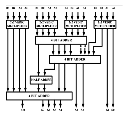
Block Diagram
Specifications
Software Requirements:
• Tanner EDA Tool (T-Spice / S-Edit)
• Technology Files: 32 nm CMOS
• SPICE Simulation Environment
Hardware Requirements:
• Microsoft® Windows 7 or above
• Intel® Core i3 Processor or equivalent
• 4 GB RAM minimum
• 500 MB of available disk space
Learning Outcomes
Introduction to Vedic Mathematics and its application in digital arithmetic
• Understanding of GDI technique and its advantages over CMOS
• Design and simulation of low-power multiplier circuits at 32 nm technology
• Analysis of Power, Delay, Area, and PDP trade-offs
• Hands-on experience with Tanner EDA simulation tools
• Circuit Design, Testing, and Debugging Skills
• Problem Analysis and Optimization Skills
• Thesis Writing and Presentation SkillsDemo Video


Request for Video
Related Projects
 Paper Publishing
Request Call Back
Would you like to receive a free callback now?
Choose the best time for callback:
Leave your message and we will contact you as soon as possible

6-2-85/B, Old Maternity Hospital Road, Thyagaraja Nagar, Tirupati, Andhra Pradesh – 517501
+91 9030333433
+91 9393939065
0877-2261612

Disclaimer - Takeoff Edu Group Projects are not associated or affiliated with IEEE in any way. The IEEE Projects mentioned here are mentioned in the context of student projects, whose ideas are derived from IEEE publications, not projects of or by IEEE.