A Modified PFD Based PLL with Frequency Dividers in 0.18-µm CMOS Technology
Also Available Domains Cadence EDA
Objective
The main objective of this project is to design an effective performance PLL using novel structure of PFD using Dynamic inverter and frequency divider structures in the the design of final PLL circuit.
Abstract
This paper introduces a modified design of CMOS dynamic Phase Frequency Detector (PFD). The proposed PFD circuit (PPFD) is designed, simulated and the results obtained are analyzed. In order to reduce dead zone, internal signal routing is used in the PPFD circuit. To extend, Phase Locked Loop (PLL) is designed and it is verified with Frequency Divider (FD) circuit. There is a decrease in area of the PLL circuit with 55 transistors and dissipates power of 89.2 pW for 1.8 V power supply. The pre-layout simulation result shows that the PPFD circuit has an elimination of a dead zone. Further, it works with the high speed and reduced power operated in the reference frequency.
Key words:-PFD, Dead Zone, VCO, Power, PLL
NOTE: Without the concern of our team, please don't submit to the college. This Abstract varies based on student requirements.
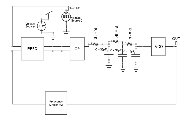
Block Diagram
Specifications
Software Requirements:
- Tool: Cadence Virtuoso
- Technology: GPDK 45nm
Hardware Requirements:
- Microsoft® Windows XP
- Intel® Pentium® 4 processor or Pentium 4 equivalent with SSE support
- 512 MB RAM
- 100 MB of available disk space
Learning Outcomes
· Introduction to Analog & Digital Electronics
· Necessity of PLL.
· Advantages & Applications of PLL.
· Basics of VCO
o Different configurations of VCO
· Knowledge on Low pass filter
· Design of PLL in Cadence
· Analysis of simulation results & Outputs
· Scope of PLL in today’s world.
· Real time applications of PLL.


 Paper Publishing

Request Call Back
Would you like to receive a free callback now?
Choose the best time for callback:
Leave your message and we will contact you as soon as possible

6-2-85/B, Old Maternity Hospital Road, Thyagaraja Nagar, Tirupati, Andhra Pradesh – 517501
+91 9030333433
+91 9393939065
0877-2261612

Disclaimer - Takeoff Edu Group Projects are not associated or affiliated with IEEE in any way. The IEEE Projects mentioned here are mentioned in the context of student projects, whose ideas are derived from IEEE publications, not projects of or by IEEE.