A Memristor-Based In-Memory Adaptive Approximate Adder
Objective
This work presents the design of a memristor-based in-memory adaptive approximate adder aimed at achieving high energy efficiency and reduced computation latency for modern computing applications. With the limitations of conventional CMOS architectures, particularly the von Neumann bottleneck caused by separate memory and processing units, in-memory computing using memristors has emerged as a promising solution
Abstract
Keywords
Memristor, In-Memory Computing, Approximate Adder, Low Power, Adaptive Design, Non-Volatile Memory, Nanoelectronics
NOTE: Without the concern of our team, please don't submit to the college. This Abstract varies based on student requirements.
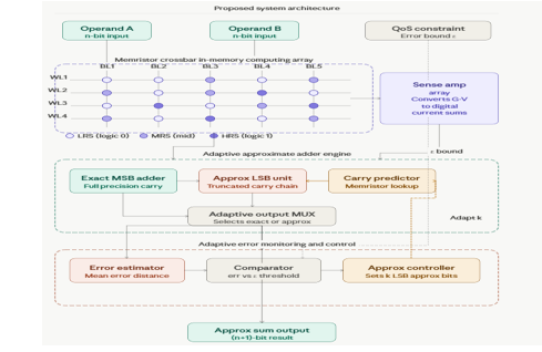
Block Diagram
Specifications
· Tool Used: Cadence EDA tools for schematic and simulation
· Technology Node:180nm CMOS process.
· Design Elements: complementary compound push–pull pair (PMOS + NMOS), input matching network, L1 & L2 (0.5 pH–10 pH) inductors, high-value output load (RL, 100 kΩ–1 MΩ), biasing/level-shift network, feedback/compensation path, input/output coupling and decoupling capacitors, thermal-stabilization circuitry, and symmetric/layout considerations for reduced mismatch
· Optimization Goal: minimize circuit complexity and parasitics (transistor and passive count) while preserving ultra-wideband large-signal gain, low output noise, high temperature stability, and linearity across the desired cutoff range (e.g., maintain cutoff from ≈18.21 kHz up to hundreds of GHz in simulation) with low power consumption (~69 mW)v
Learning Outcomes
Understanding of Memristor Technology
• Knowledge of In-Memory Computing Architecture
• Design of Approximate Adders
• Trade-off Analysis Between Accuracy and Efficiency
• Low-Power Nanoelectronic Circuit Design
• Exposure to Emerging Computing Paradigms


 Paper Publishing

Request Call Back
Would you like to receive a free callback now?
Choose the best time for callback:
Leave your message and we will contact you as soon as possible

6-2-85/B, Old Maternity Hospital Road, Thyagaraja Nagar, Tirupati, Andhra Pradesh – 517501
+91 9030333433
+91 9393939065
0877-2261612

Disclaimer - Takeoff Edu Group Projects are not associated or affiliated with IEEE in any way. The IEEE Projects mentioned here are mentioned in the context of student projects, whose ideas are derived from IEEE publications, not projects of or by IEEE.