A Low-Power and High-Speed Voltage Level Shifter Based on a Regulated Cross-Coupled Pull-Up Network
Also Available Domains Low Power VLSI|Tanner EDA|Cadence EDA
Abstract
Abstract:
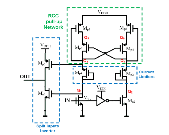
In this project, a high speed and low power voltage level shifter (LS) is presented. By using a new regulated cross-coupled (RCC) pull-up network, the switching speed is boosted and the dynamic power consumption is highly reduced. The proposed (LS) has the ability to convert input signals with voltage levels 0.6 to output voltage level 1.8. The presented LS occupies a small silicon area owing to its very low number of elements and is ultra-low-power, making it suitable for low-power applications such as implantable medical devices and wireless sensor networks.
NOTE: Without the concern of our team, please don't submit to the college. This Abstract varies based on student requirements.
Block Diagram
Specifications
Specifications:
Software Requirements:
· Tanner EDA
· Technology files:45nm
Hardware Requirements:
· Microsoft® Windows XP
· Intel® Pentium® 4 processor or Pentium 4 equivalent with SSE support
· 512 MB RAM
· 100 MB of available disk space
Learning Outcomes
Learning Outcomes:
- Introduction to Level shifters
- Multi voltage designs
- Introduction to current limiters
- Transistors & its applications
o Types of Transistors
o Logic Gates using Transistors
o Pull Up and Pull Down networks
o Importance of Transistors
- MOS Fundamentals
- NMOS/PMOS/CMOS Technologies
- How to design circuits using Transistor logic?
- Transistor level design for analog to digital converters
- How to design low power, high speed area efficient transistor level circuits?
- Importance of Static power consumption
- Techniques for reducing static power consumption
- Scope of Level shifters in today’s world
- Applications in real time
Demo Video


Request for Video
 Paper Publishing
Request Call Back
Would you like to receive a free callback now?
Choose the best time for callback:
Leave your message and we will contact you as soon as possible

6-2-85/B, Old Maternity Hospital Road, Thyagaraja Nagar, Tirupati, Andhra Pradesh – 517501
+91 9030333433
+91 9393939065
0877-2261612

Disclaimer - Takeoff Edu Group Projects are not associated or affiliated with IEEE in any way. The IEEE Projects mentioned here are mentioned in the context of student projects, whose ideas are derived from IEEE publications, not projects of or by IEEE.