A High-Speed and Power-Efficient Voltage Level Shifter for Dual-Supply Applications
Also Available Domains Low Power VLSI|Tanner EDA
Abstract
NOTE: Without the concern of our team, please don't submit to the college. This Abstract varies based on student requirements.
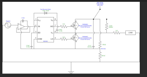
Block Diagram
Specifications
System Configuration:-
In the hardware part a normal computer where T-spice software can be easily operated is required, i.e., with a minimum system configuration
Hardware requirement
Processor - Pentium –III
Speed - 1.1 GHz
RAM - 1 GB (min)
Hard Disk - 40 GB
Floppy Drive - 1.44 MB
Key Board - Standard Windows Keyboard
Mouse - Two or Three Button Mouse
Monitor - SVGA
Software requirements
v Operating System :Windows95/98/2000/XP/Windows7
v Tools : Tanner EDA
Learning Outcomes
Understanding of Voltage Level Shifting Techniques: The paper would provide insights into different voltage level shifting techniques used in electronic circuits to interface between different voltage domains. Learners will understand the challenges and considerations involved in designing level shifters for dual-supply applications.
Knowledge of Dual-Supply Circuit Design: Learners will gain knowledge about dual-supply circuit design and the importance of using voltage level shifters to enable communication between different voltage domains in a system.
High-Speed Design Techniques: The paper may discuss various high-speed design techniques used to improve the performance of the voltage level shifter. Learners will understand the trade-offs between speed, power efficiency, and area.
Power-Efficient Design Principles: The paper is likely to highlight power-efficient design principles that help reduce power consumption in the voltage level shifter. Learners will be exposed to techniques to minimize power dissipation while maintaining reliable signal integrity.
Analyzing Research Papers: By studying this paper, learners will develop skills in critically analyzing research papers, understanding the methodologies used, and evaluating the results and conclusions presented.
Knowledge of CMOS Technology: The paper may delve into CMOS technology, which is commonly used for implementing voltage level shifters and other digital circuits. Learners will gain insights into the operation and characteristics of CMOS transistors.
Applying Concepts to Practical Design: Learners may gain the ability to apply the concepts presented in the paper to design their voltage level shifters for specific dual-supply applications or incorporate the ideas into larger electronic systems.
Understanding Trade-offs in Circuit Design: Learners will learn to weigh the trade-offs between various parameters such as speed, power consumption, area, and voltage range while designing voltage level shifters for dual-supply applications.
Awareness of Circuit Implementation Challenges: Learners will become aware of the challenges faced when implementing high-speed and power-efficient voltage level shifters, such as signal integrity issues, parasitic capacitances, and technology limitations.
Awareness of Current Research Trends: The paper may include references to other related research works, allowing learners to explore current research trends and advancements in voltage level shifting and dual-supply circuit design.


 Paper Publishing

Request Call Back
Would you like to receive a free callback now?
Choose the best time for callback:
Leave your message and we will contact you as soon as possible

6-2-85/B, Old Maternity Hospital Road, Thyagaraja Nagar, Tirupati, Andhra Pradesh – 517501
+91 9030333433
+91 9393939065
0877-2261612

Disclaimer - Takeoff Edu Group Projects are not associated or affiliated with IEEE in any way. The IEEE Projects mentioned here are mentioned in the context of student projects, whose ideas are derived from IEEE publications, not projects of or by IEEE.