A Circuit Technique for Leakage Power reduction in CMOS VLSI Circuits
Objective
In this work, we address the issue of leakage power that arises with the device channel length scaling to sub-100nm. We present a circuit technique to mitigate the leakage currents of MOSFET through controlling the voltage at the source terminal of the MOSFET.
Abstract
Abstract:
This paper presents a circuit technique aimed at reducing leakage power in CMOS VLSI circuits. With the advancement of CMOS technology, leakage currents have become a significant concern, especially in the ultra-deep-submicron region. Minimizing leakage currents is crucial to ensure proper circuit operation. Designing nanoscale CMOS circuits that are free from leakage poses a formidable challenge. In this study, we propose a circuit technique that effectively controls the voltage at the source terminal of MOSFETs to mitigate leakage currents. By employing this technique, we observe a significant improvement in static power dissipation and overall power consumption in the designed CMOS inverter compared to conventional designs. Furthermore, simulation results demonstrate enhanced power efficiency in NAND and NOR gates implemented using the same approach, as well as in an 11-stage CMOS ring oscillator. A comparison with existing techniques considering power dissipation and delay is also provided, highlighting the favorable Power-Delay Product (PDP) achieved by the proposed circuits. The findings of this study indicate the potential of the proposed technique for reducing leakage power and improving power efficiency in CMOS VLSI circuits.
NOTE: Without the concern of our team, please don't submit to the college. This Abstract varies based on student requirements.
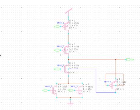
Block Diagram
Specifications
Software Requirements:
· Tanner tool
· Technology files: 45nm
Hardware Requirements:
· Microsoft® Windows XP
· Intel® Pentium® 4 processor or Pentium 4 equivalent with SSE support
· 512 MB RAM
· 100 MB of available disk space
Learning Outcomes
Learning Outcomes:
- Introduction to Digital electronics
- Importance of Transistors
- MOS Fundamentals
- NMOS/PMOS/CMOS Technologies
- How to design circuits using Transistor logic?
- Scope of multipliers in today’s world
- Applications in Real time.
- Tanner tool for design and simulation
- Solution providing for real time problems
- Project Development Skills:
- Problem Analysis Skills
- Problem Solving Skills
- Logical Skills
- Designing Skills
- Testing Skills
- Debugging Skills
- Presentation skills
- Thesis Writing Skills
Demo Video


Request for Video
 Paper Publishing
Request Call Back
Would you like to receive a free callback now?
Choose the best time for callback:
Leave your message and we will contact you as soon as possible

6-2-85/B, Old Maternity Hospital Road, Thyagaraja Nagar, Tirupati, Andhra Pradesh – 517501
+91 9030333433
+91 9393939065
0877-2261612

Disclaimer - Takeoff Edu Group Projects are not associated or affiliated with IEEE in any way. The IEEE Projects mentioned here are mentioned in the context of student projects, whose ideas are derived from IEEE publications, not projects of or by IEEE.