A 21-Transistor Single-Phase-Clocked Flip-Flop With Low Leakage Current for Near-Threshold Voltage Operation
Objective
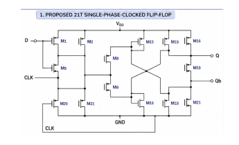
This work presents the design and implementation of a 21-transistor (21T) single-phase-clocked flip-flop optimized for low leakage current operation under near-threshold voltage conditions. As modern digital systems increasingly demand ultra-low power consumption for portable and energy-constrained applications, operating circuits at near-threshold voltages has become an effective strategy
Abstract
This work presents the design and implementation of a 21-transistor (21T) single-phase-clocked flip-flop optimized for low leakage current operation under near-threshold voltage conditions. As modern digital systems increasingly demand ultra-low power consumption for portable and energy-constrained applications, operating circuits at near-threshold voltages has become an effective strategy. However, conventional flip-flop designs suffer from increased leakage current, reduced speed, and reliability issues at such low supply voltages.
The proposed flip-flop utilizes a single-phase clocking scheme to simplify clock distribution and reduce dynamic power consumption. The 21T architecture is carefully designed to minimize leakage paths while maintaining robust data retention and switching performance. Techniques such as transistor stacking, optimized sizing, and efficient feedback mechanisms are employed to enhance stability and reduce power dissipation.
The design is implemented using CMOS technology and evaluated in terms of power consumption, leakage current, delay, and power-delay product (PDP). Simulation results demonstrate that the proposed flip-flop achieves significantly reduced leakage current and improved energy efficiency while maintaining reliable operation at near-threshold voltages, making it suitable for low-power VLSI systems.
Keywords
Flip-Flop, Single-Phase Clocking, Low Leakage, Near-Threshold Voltage, CMOS, Low Power, VLSI Design
NOTE: Without the concern of our team, please don't submit to the college. This Abstract varies based on student requirements.
Block Diagram
Specifications
· Tool Used: Cadence EDA tools for schematic and simulation
· Technology Node:180nm CMOS process.
· Design Elements: complementary compound push–pull pair (PMOS + NMOS), input matching network, L1 & L2 (0.5 pH–10 pH) inductors, high-value output load (RL, 100 kΩ–1 MΩ), biasing/level-shift network, feedback/compensation path, input/output coupling and decoupling capacitors, thermal-stabilization circuitry, and symmetric/layout considerations for reduced mismatch
· Optimization Goal: minimize circuit complexity and parasitics (transistor and passive count) while preserving ultra-wideband large-signal gain, low output noise, high temperature stability, and linearity across the desired cutoff range (e.g., maintain cutoff from ≈18.21 kHz up to hundreds of GHz in simulation) with low power consumption (~69 mW)v
Learning Outcomes
Understanding of Flip-Flop Design
• Knowledge of Low-Power Design Techniques
• Application of Near-Threshold Computing
• Leakage Reduction Methods (Transistor Stacking)
• Performance Analysis Using PDP
• Experience with CMOS Circuit Simulation
Demo Video


Request for Video
 Paper Publishing
Request Call Back
Would you like to receive a free callback now?
Choose the best time for callback:
Leave your message and we will contact you as soon as possible

6-2-85/B, Old Maternity Hospital Road, Thyagaraja Nagar, Tirupati, Andhra Pradesh – 517501
+91 9030333433
+91 9393939065
0877-2261612

Disclaimer - Takeoff Edu Group Projects are not associated or affiliated with IEEE in any way. The IEEE Projects mentioned here are mentioned in the context of student projects, whose ideas are derived from IEEE publications, not projects of or by IEEE.