45nm CMOS 4-Bit Flash Analog to Digital Converter
Also Available Domains Low Power VLSI|Cadence EDA|Tanner EDA
Objective
The main objective of this paper is to reduce the power in ADC. The design of ADC describes an effective method to reduce area and power consumption
Abstract
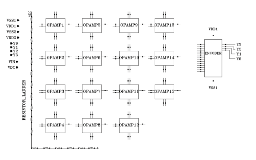
In this project, a 4-bit flash ADC is designed using CMOS 45nm technology. Signal processing and communication systems are widely dependent on the Analog to Digital Converters (ADC). Operational amplifier design, which remains as the integral part of ADC is also discussed.
To enable an improved performance of the ADC, the operational amplifier is designed with a frequency range 5MHz along with an operating voltage of 2.5 which produces a thermometer code. Finally the thermometer encoder circuit is used to convert the thermometer code to binary output. All the designs are implemented using 45nm technology in Cadence Virtuoso.
Keywords: Flash ADC, 45nm, CMOS, Op-Amp.
NOTE: Without the concern of our team, please don't submit to the college. This Abstract varies based on student requirements.
Block Diagram
Specifications
Software Requirements:
- Cadence Virtuoso
- Technology files: 45 nm
Hardware Requirements:
- Microsoft® Windows XP
- Intel® Pentium® 4 processor or Pentium 4 equivalent with SSE support
- 512 MB RAM
- 100 MB of available disk space

Demo Video


Request for Video
Related Projects
 Paper Publishing
Request Call Back
Would you like to receive a free callback now?
Choose the best time for callback:
Leave your message and we will contact you as soon as possible

6-2-85/B, Old Maternity Hospital Road, Thyagaraja Nagar, Tirupati, Andhra Pradesh – 517501
+91 9030333433
+91 9393939065
0877-2261612

Disclaimer - Takeoff Edu Group Projects are not associated or affiliated with IEEE in any way. The IEEE Projects mentioned here are mentioned in the context of student projects, whose ideas are derived from IEEE publications, not projects of or by IEEE.