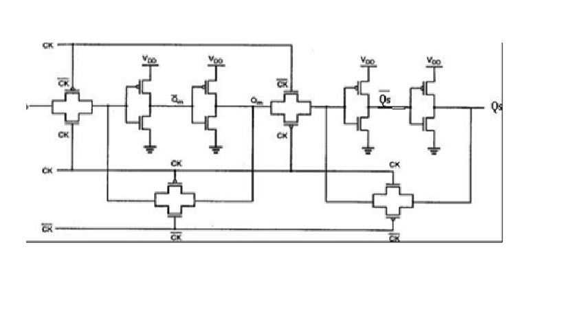
Power Efficient Clock Pulsed D Flip Flop Using Transmission Gate
Objective
The main aim of this project is to implement the clock pulsed D flip flop using Transmisson gate to reduce the power
Abstract
The need for low-power sequential circuits is pushing towards the implementation of low power consuming basic memory elements like D Flip-Flop. To accomplish power efficient D Flip-Flop, 180 nm CMOS technology is utilized to develop a novel eminent performance Current-Mode Pulse Triggered D Flip-Flop. Instead of voltage utilization in clock distribution is the new idea in the developed method uses current to render low power consumption clock signal. D Flip-Flop is designed by transmission gate which is also reduces the power consumption along with Current-Mode signaling. The Tanner/LT spice/Cadence - Virtuoso tool is to be used to simulate all the circuits with 180nm technology. Power consumption reduction in the designed D Flip-Flop is the foremost and major aim of the project. For reducing, power consumption in D Flip-Flop we are employing two methods. They are, Use of Current Mode Clock Distribution Networks (CM-CDN) instead of Voltage Mode ClockFlop, instead of cmos logic.
NOTE: Without the concern of our team, please don't submit to the college. This Abstract varies based on student requirements.
Block Diagram

Specifications
Software Requirements:
· Tool: Tanner EDA/Cadence Virtuoso
· Technology: 45nm.
Hardware Requirements:
- Microsoft® Windows XP
- Intel® Pentium® 4 processor or Pentium 4 equivalent with SSE support
- 512 MB RAM
- 100 MB of available disk space
Learning Outcomes
· Understanding Clocking Techniques
· Power Optimization Techniques
· Advantages and Applications
· Low-Power Design Principles.
· Timing Analysis and Performance Optimization
· Tool Learning in Tanner EDA/Cadence Virtuoso
· Analysis of design and simulation results
· Noise Immunity and Signal Integrity


 Paper Publishing
