An Efficient TDC Using a Dual-Mode Resource-Saving Method Evaluated in a 28-nm FPGA
Also Available Domains Arithmetic Core|Xilinx Vivado
Objective
The main aim of this paper is to implement the time-to-digital-converter (TDC) based on the dual-mode tapped delay line using CARRY4 sequence to reduce the dead-time.
Abstract
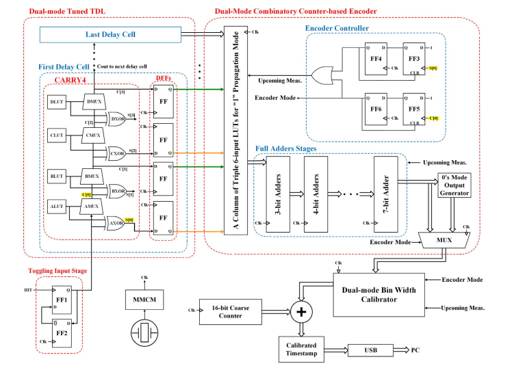
FPGA-based time-to-digital converters (TDCs) are required to be accurate, linear, and fast, while at the same time employing a reduced number of resources. Pushing these requirements to the limit is challenging, although it is constantly required by many applications. This article presents a dual-mode tapped-delay-line (TDL)—propagating 1’s and 0’s in alternating measurement cycles—architecture for a field-programmable gate array (FPGA)-based TDC that complies with the mentioned specifications. The dead-time of the proposed TDC is reduced to one system clock cycle by using a toggling input stage and a dual-mode counter-based encoder. To improve the TDC linearity, the TDL sampling sequence is tuned separately for each operating mode. The presented architecture employs a low-resources dualmode combinatory encoder of one- and zero-counters to remove the bubbles and cover both operating modes. A dual-mode binwidth calibration has been carried out to improve the TDC performance in each mode. The proposed architecture has been implemented on a Xilinx Artix-7 FPGA.
NOTE: Without the concern of our team, please don't submit to the college. This Abstract varies based on student requirements.
Block Diagram

Specifications
Software Requirements:
· Xilinx ISE Tool
· HDL: Verilog
Hardware Requirements:
· Microsoft® Windows XP,
· Intel® Pentium® 4 processor or Pentium 4 equivalent with SSE support
· 512 MB RAM
· 100 MB of available disk space
Learning Outcomes
- Basics of Digital Electronics
- FPGA design Flow
- Introduction to Verilog Coding
- Different modeling styles in Verilog
o Data Flow modeling
o Structural modeling
o Behavioral modeling
o Mixed level modeling
- Concept of Distributed Arithmetic based Filter
- Importance of TDC using a dual-mode resource
- Drawbacks of TDC
- Introduction to FPGA-based TDCs
- Knowledge on minimizing the use of resources and power consumption.
- Applications of TDC
- Scope of filters concept in today’s world
- Applications in real time
- Xilinx ISE 14.7 for design and simulation
- Generation of Net list
- Solution providing for real time problems
- Project Development Skills:
o Problem Analysis Skills
o Problem Solving Skills
o Logical Skills
o Designing Skills
o Testing Skills
o Debugging Skills
o Presentation Skills
o Thesis Writing Skills


 Paper Publishing
