A Unified NVRAM and TRNG in Standard CMOS Technology
Also Available Domains Tanner EDA
Objective
The main objective of this project is to present a NVRAM TRNG using a novel mechanism to manage the charges into SFG.
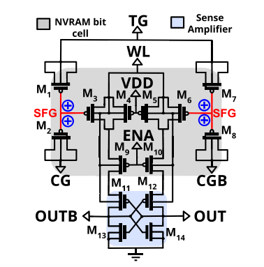
Block Diagram
Specifications
Software Requirements:
· CADENCE VIRTUOSO
· Technology files: 45nm
Hardware Requirements:
· Microsoft® Windows XP
· Intel® Pentium® 4 processor or Pentium 4 equivalent with SSE support
· 512 MB RAM
· 100 MB of available disk space
Learning Outcomes
Learning Outcomes:
- Introduction to NVRAM
- Need of NVSRAM in IOT applications
- Transistors & its applications
o Types of Transistors
o Logic Gates using Transistors
o Pull Up and Pull Down networks
o Importance of Transistors
- MOS Fundamentals
- NMOS/PMOS/CMOS Technologies
- How to design circuits using Transistor logic?
- Transistor level design for NVRAM
- How to design low power, high speed area efficient transistor level circuits?
- Drawbacks in CMOS technology
- Scope of NVRAM & Cryptography in today’s world
- Applications in real time
· CADENCE VIRTUOSO tool for design and simulation
- Solution providing for real time problems
· Project Development Skills:
o Problem Analysis Skills
o Problem Solving Skills
o Logical Skills
o Designing Skills
o Testing Skills
o Debugging Skills
o Presentation skills
o Thesis Writing Skills


 Paper Publishing

Request Call Back
Would you like to receive a free callback now?
Choose the best time for callback:
Leave your message and we will contact you as soon as possible

6-2-85/B, Old Maternity Hospital Road, Thyagaraja Nagar, Tirupati, Andhra Pradesh – 517501
+91 9030333433
+91 9393939065
0877-2261612

Disclaimer - Takeoff Edu Group Projects are not associated or affiliated with IEEE in any way. The IEEE Projects mentioned here are mentioned in the context of student projects, whose ideas are derived from IEEE publications, not projects of or by IEEE.